
1987
1.
In the figure, if the CMRR of the
operational amplifier is 60 dB, then the magnitude of the output voltage is

Answer: 100 mV
1988
1.
The OP-AMP shown in figure below is
ideal and R = (L/C)1/2. The phase angle between Vo and Vi at ω = 1/(LC)1/2
is

a. π/2
b. π
c. 3π/2
d. 2π
Answer: C
1989
1.
Referring to the figure shown,

Answer: B & C
1990
1.
The operational amplifier has a very
poor open loop gain of 45, otherwise is ideal. The gain of the amplifier is

a. 5
b. 20
c. 4
d. 4.5
Answer: D
2.
The CMRR of the differential
amplifier shown is

a. Infinity
b. Zero
c. 900
d. 1800
Answer: C
3.
If the input to the circuit shown is
a sine wave, the output will be

a. Half wave rectified sine wave
b. Full wave rectified sine wave
c. Triangular wave
d. Square wave
Answer: D
1991
1.
In order that the circuit of figure
works properly as differentiator it should be modified to __________(draw the
modified circuit)

2.
In the figure, the operational
amplifier is ideal and its output can swing between – 15 and + 15 volts.

The
input Vi, which is zero for t<0, is switched to 5 volts at the
instant t = 0. Given that the output Vo is + 15 volts for t<0,
sketch the waveforms of Vo and Vi. You must give the
values of important parameters of the sketch.
3.
In figure, the operational amplifier
are ideal and their output can swing between – 15 and + 15 volts. Sketch the
waveform of voltages of V1 and V2 as a function of time.
You must give the values of important parameters of this sketch.


1992
1.
An operational amplifier has an
offset voltage of 1 mV and is ideal in all other respects. If this amplifier is
used in the circuit shown in figure, the output voltage will be (select the
nearest value)
a. 1 mV
b. 1 V
c. ± 1 V
d. 0

Answer: C
2.
The circuit of figure uses an ideal
operational amplifier. For small positive values of Vin, the circuit
works as

a. Half Wave Rectifier
b. Differentiator
c. Logarithmic amplifier
d. Exponential amplifier
Answer: C
3.
Assume that the operational
amplifier in figure is ideal. The current I through the 1 kΩ resistor is _____________

Answer: - 4 mA
4.
The transistors in the differential
amplifier shown in figure are identical with hfe = 100 and re
= 25 Ω
at 1 mA collector current. The circuit has a CMRR of 100.
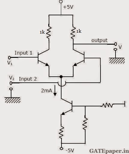
a. What is the differential gain of the circuit?
b. What is the common mode gain of the circuit?
c. If DC voltage of 1010 mV and 990 mV are applied to inputs 1
and 2 respectively with reference to
ground, what will be the output voltage Vo?
5.
Consider the circuit shown in
figure. This circuit uses an ideal operational amplifier.

Assuming that the impedance's at nodes A and B do not load the
preceding bridge circuit, calculate the output voltage Vo. When
(a) RA = RB = RC
= RD = 100 Ω and (b) RA = RB = RC
= 100 Ω and RD = 120 Ω.
1993
1.
For the ideal operational amplifier
circuit shown, determine the output voltage Vo.

Answer: 20 mV
Solution : https://www.youtube.com/watch?v=Bs47-UqAHLo
2. Find the output voltage Vo in the following
circuit, assuming that the operational amplifier is ideal.

1994
1.
The frequency compensation is used
in operational amplifiers is to increase its ___________
Answer: Stability
2. Assuming that the amplifier shown in the figure below is a
voltage controlled voltage source.
Show that the voltage transfer function of the network is given by
Show that the voltage transfer function of the network is given by

3. Calculate the frequency at which zero transmission is
obtained from the Wien-bridge shown below.

4. Find the output voltage of the following circuit shown
below, assuming ideal operational amplifier behavior.

1995
1.
A change in the value of the emitter
resistance, RE, in a differential amplifier
a. affects the difference mode gain Ad
b. affects the common mode gain Ac
c. affects both Ad and Ac
d. does not affect both Ad and Ac.
Answer: B
2.
In the given circuit, if the voltage
V+ and V_ are to amplified by the same factor, the value
of R should be _________

Answer: 33 kΩ
3.
An OP-AMP is used as a zero crossing
detector. If the maximum output available from the OP-AMP is ±12 volts peak to peak, and the slew rate of the OP-AMP is 12
V/µsec,
then the maximum frequency of the input signal that can be applied without
causing a reduction in the peak to peak output is _____________
Answer: 1.59 KHz
4. Sketch the output as a function of the input voltage (for
negative values) for circuit shown below. Assume ideal operational amplifier
and diode forward voltage drop as zero.

5. The waveform input to the sweep generator circuit shown in
figure, is a square wave of period 2 msec and amplitude varying between 0 and
12 volts.

a. Draw the waveform Vo(t), in relation to the input
b. Specify Vo(t) determine the voltage levels and
the time constants involved.
6. Show that the circuit shown in figure is double integrator.
In other words, prove that the transfer gain is given by Vo(s)/Vs(s)
= 1/(CRs)2, assume
ideal operational amplifier.

1996
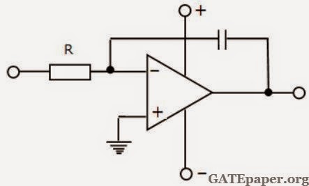
1.
The circuit shown in the figure
is that of

a. A Non-inverting amplifier
b. An Inverting amplifier
c. An Oscillator
d. A Schmitt trigger
Answer: D
2.
Value of R in the oscillator circuit
shown in the given figure, so chosen that it just oscillates at an angular
frequency of ω.
The value of ω
and the required value of R will respectively are

a. 105 rad/sec, 2 x 10⁴ Ω
b. 2 x 10⁴ rad/sec, 2 x 10⁴ Ω
c. 2 x 10⁴ rad/sec,
105 Ω
d. 105 rad/sec,
105 Ω
Answer: A
3. A resistively loaded and resistively biased differential
amplifier circuit is shown. Neglect base current and assume matched transistors
with VA -> ∞
and β
= 100. Use VT = 26 mV, VBE(on) = 0.7 volts and VCE(sat)
= 0.1 volts.

a. Determine the values of RC and R2 to
meet the following specifications: double ended differential mode gain = 500,
CMRR = 500 and differential mode input resistance of 2 MΩ.
b. Determine the minimum values of VCC and VEE
such that the transistors remain in the forward active region under zero signal
condition. Assume that the DC common mode input is zero.
Answer: (a) 5 MΩ, 2.5 MΩ (b) 12.6 Volts, -13.83 Volts
Solution: https://www.youtube.com/watch?v=9zaM7i-wdmI
4. Assuming ideal operational amplifiers, show that the circuit
shown simulates in inductor i.e. show that Vi(S)/Ii(S) is
inductive and write the expression for the effective inductance.
1997
1.
The output voltage Vo of
the circuit shown is

a. – 4 volts
b. 6 volts
c. 5 volts
d. – 5.5 volts
Answer: D
2.
Consider the circuit given in the
figure is using an ideal operational amplifier. The characteristics of the diode are given by the relation I =
IS(eqV/KT – 1), where V is the forward voltage across
the diode.

a.
Express Vo as function of
Vi , assuming Vi > 0
b. If R = 100 kΩ, IS = 1 µA and VT = 25
mV, find the input voltage Vi for which Vo = 0.
Answer: (a) VD = ISR – VT ln(Vi/ISR) (b) 5.46 Volts
Solution: https://www.youtube.com/watch?v=uuBa60badBA
3.
In circuit shown, assume that the
operational amplifier is ideal and that Vo = 0 volts initially. The switch is connected first to ‘A’ charging
C1 to the voltage V. it is then connected to the point ‘B’. This
process is repeated 'f' times per second.

a.
Calculate the charge transferred per
second from node A to node B.
b.
Derive the average rate of change of
the output voltage Vo.
c.
If the capacitor and the switch are
removed and a resistor is connected between
points A and B, find the value of the resistor to get the same average
rate of change of the
output voltage?
d.
If the repetition rate of the
switching action is 104 times per second, C1 = 100pF, C2
= 10pF and V= 10 mV. What is the average change of the output voltage?
Answer: (a) C1Vf (b) – (C1Vf)/C2 (c) R = 1/C1f (d) - 1000 V/sec
Solution: https://www.youtube.com/watch?v=5lfnNxFBP8M
4. An IC 555 chip has been used to construct a pulse generator.
Typical pin connections with components are
shown below. It is desired to generate a square pulse of 10 kHz.

Evaluate values of RA and RB
if the capacitor C has the value of 0.01 µF for the configuration
chosen. If necessary you can suggest modification in the external configuration.
1998
1.
In a differential amplifier, CMRR
can be improved by using an increased
a. Emitter resistance
b.
Collector resistance
c.
Power supply voltages
d.
Source resistance
Answer: A
2.
From a measurement of the rise time
of the output pulse of an amplifier, whose input is a small amplitude square
wave, one can estimate the following parameter of the amplifier
a.
Gain-bandwidth product
b.
Slew rate
c.
Upper 3 dB frequency
d.
Lower 3 dB frequency
Answer: C
3.
The emitter coupled pair of BJT’s
given a linear transfer relation between the differential output voltage and
the differential input voltage Vid, only when the magnitude of Vid is less α times the thermal voltage, where α is
a.
4
b.
3
c.
2
d.
1
Answer: A
4. One input terminal of high gain comparator circuit is
connected to ground and a sinusoidal voltage is applied to the other input. The
output of comparator will be
a. A sinusoid
b.
A full rectified sinusoid
c.
A half rectified sinusoid
d.
A square wave
Answer: D
5. Determine the input impedance of the circuit shown and
investigate if it can be inductive.

Answer: Zi = - R2(1+SCR1)/(1+SCR2) and Zi is not Inductive.
Solution: https://www.youtube.com/watch?v=XU0TAARC8ek
6. Find the value of R’ in the circuit shown for generating
sinusoidal oscillations. Find the frequency of oscillations.

7. Implement a monostable multivibrator using the timer circuit
shown in figure. Also determine an expression for ON time ‘T’ of the output
pulse.

1999
1.
The first pole encountered in the
frequency response of a compensated OP-AMP is approximately at
a. 5 Hz
b. 10 kHz
c. 1 MHz
d. 100 MHz
Answer: A
2. Neatly sketch and label the DC transfer characteristic (Vo
verses Vin) of the circuit shown, as Vin varies from – 2
volts to + 2 volts.

Assume ideal operational amplifier and the diodes have a forward voltage of 0.6
volts and zero incremental resistance.
2000
1.
In the differential amplifier of the
figure, if the source resistance of the current source IEE is
infinite, then the common mode gain is

a. Zero
b. Infinite
c. Indeterminate
d. (Vin1 + Vin2) / 2VT
Answer: A
2.
In the circuit shown in figure, the
output voltage Vo is

a. – 1 volts
b. 2 volts
c. + 1 volts
d. + 15 volts
Answer: D
3.
If the OP-AMP in the figure is ideal,
then the output voltage Vo is
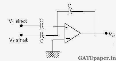
a. Zero
b. (V1 – V2) sinωt
c. – (V1 + V2) sinωt
d. (V1 + V2) sinωt
Answer: C
4.
The configuration of the figure is
a

a. Precision rectifier
b. Hartley oscillator
c. Butterworth high pass filter
d. Wien-bridge oscillator
Answer: D
5.
Assume that the OP-AMP of the figure
is ideal. If Vi is a triangular wave, then Vo will be

a. Square wave
b. Triangular wave
c. Parabolic wave
d. Sine wave
Answer: A
6.
The most commonly used amplifier in
Sample and Hold circuits is
a. Unity gain inverting amplifier
b. Unity gain non-inverting amplifier
c. An inverting amplifier with a gain of 10
d. An inverting amplifier with a gain of 100
Answer: B
7.
If the OP-AMP in the figure has an
input offset voltage of 5 mV and an open loop voltage gain of 10,000. Then the
output Vo will be

a. 0 volts
b. 5 mV
c. + 15 volts or – 15 volts
d. + 50 volts or – 50 volts
Answer: C
No comments:
Post a Comment