2001
1.
The ideal OP-AMP has the following
characteristics
a. Ri = ∞, AV= ∞, Ro = 0
b. Ri = 0, AV= ∞, Ro = 0
c. Ri = ∞, AV= ∞, Ro = ∞
d. Ri = 0, AV= ∞, Ro = ∞
Answer: A
2.
The inverting OP-AMP shown in the
figure has an open loop gain of 100. The closed loop gain Vo/Vs
is
a. – 8
b. – 9
c. – 10
d. – 11
Answer: B
3.
In the figure, assume the OP-AMPs to
be ideal. The output Vo of the circuit is
4. In the circuit shown, assume that the OP-AMP is ideal.
a. Obtain an expression for Vo in terms of Vs,
R and the reverse saturation current Is of the transistor.
b. If R = 1 Ω,
Is = 1 pA and the thermal voltage VT = 25 mV, then what
is the value of the output voltage Vo for an input voltage Vs
of 1 volt?
c. Suppose that the transistor in the feedback path is replaced
by a PN junction diode with a reverse
saturation current of Is. The P-side of the diode is connected to
node A and the N-side to node B. then what is the expression for Vo
in terms of Vs, R and Is ?
2002
1.
A 741 OP-AMP has a gain-bandwidth
product of 1 MHz. A non-inverting amplifier using this OP-AMP and having a
voltage gain of 20 dB will exhibit a –3 dB bandwidth of
a. 50 kHz
b. 100 kHz
c. 100/17 kHz
d. 1000/7.07 kHz
2.
The circuit in the figure employs
positive feedback and is intended to generate sinusoidal oscillations. If at a
frequency fo, β(f)
= Vf(f)/Vo(f) = 1/6 ∟0o, then to sustain oscillations at this
frequency
a. R2 = 6R1
b. R2 = 5R1
c. R2 = R1/6
d. R2 = R1/5
3.
An amplifier using an OP-AMP with a
slew rate SR = 1 V/µsec
has a gain of 40 dB. If this amplifier has to faithfully amplify sinusoidal
signals form dc to 20 kHz without any slew rate induced distortion, then the
input signal level must not exceed
a. 795 mV
b. 395 mV
c. 79.5 mV
d. 39.5 mV
4. Consider the circuit shown. Assume the operational amplifier
is ideal.
a. In which mode is the BJT operating (active or saturation or
cutoff)? Justify your answer.
b. Obtain an expression relating the output current Io
and the input voltage Vi.
c. Determine Io and Vop if Vi = 2 volt.
Assume β
= 99 and VBE = 0.7 volts.
Answer:
(a) Active region
(b) Vi = IORL – 15
(c) IO = 1.7 Amp, VOP = 5.25 volts
2003
1.
If the input to the ideal comparator
shown in the figure is a sinusoidal signal of 8 volts peak to peak, without any
DC component, then the output of the comparator has a duty cycle of
a. 1/2
b. 1/3
c. 1/6
d. 1/2
2.
If the differential voltage gain and
the common mode voltage gain of a differential amplifier are 48 dB and 2 dB
respectively, then common mode rejection ratio is
a. 23 dB
b. 25 dB
c. 46 dB
d. 50 dB
3.
The oscillator circuit shown in the
figure has an ideal inverting amplifier. Its frequency of oscillation in Hertz
is
4.
The output voltage of the regulated
power supply shown in the figure is
a. 3 volts
b. 6 volts
c. 9 volts
d. 12 volts
5. If the OP-AMP in the figure is ideal, the output voltage VOUT
will be equal to
a. 1 volt
b. 6 volts
c. 14 volts
d. 17 volts
2004
1.
An ideal OP-AMP is an ideal
a. Voltage Controlled Current Source
b. Voltage Controlled Voltage Source
c. Current Controlled Current Source
d. Current Controlled Voltage Source
2.
The circuit in the figure is a
a. Low pass filter
b. High pass filter
c. Band pass filter
d. Band reject filter
3. The value of capacitor C required
for sinusoidal oscillations of frequency 1 kHz in the circuit of the figure is
4. in the OP-AMP circuit given in the
figure, the load current iL is
a. – VS / R2
b. VS / R2
c. – VS / RL
d. VS / R1
2005
1.
The input resistance Ri
of the amplifier shown in figure is
a. 30/4 KΩ
b. 10 KΩ
c. 40 KΩ
d. Infinite
2.
The voltage eo indicated
in figure has been measured by an ideal voltmeter, which of the following can
be calculated?
a. Bias current of the inverting input only
b. Bias current of the inverting and non-inverting inputs only
c. Input offset current only
d. Both the bias currents and the input offset current.
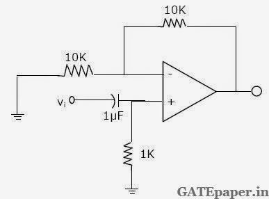
3.
The OP-AMP circuit shown in figure
is a filter. The type of filter and its cut-off frequency are respectively.
a. High pass, 1000 rad/sec
b. Low pass, 1000 rad/sec
c. High pass, 10000 rad/sec
d. Low pass, 10000 rad/sec
4.
In the differential amplifier shown
in figure, a large value of RE
a. Increases both the differential and common mode gains
b. Increases the common mode gain only
c. Decreases the differential mode gain only
d. Decreases the common mode gain only
5. Given the ideal operational amplifier circuit shown in
figure indicate the correct transfer characteristics assuming ideal diodes with
zero cut-in voltage.
2006
1.
For the circuit shown in the
following figure, the capacitor C is initially uncharged. At t = 0, the switch
S is closed. The voltage VC across the capacitor at t = 1 ms is
_____. Assume the OP – AMP is supplied with ± 15 volts.
a. 0 volts
b. 6.3 volts
c. 9.45 volts
d. 10 volts
Statement
for Linked Answer Questions (2 and 3):
A regulated power supply shown in
the figure below has an unregulated input of 15 volts and generates a regulated
output Vout. Use the component values shown in the figure.
2. The power dissipation across the transistor Q1
shown in the figure is
a. 4.8 volts
b. 5.0 volts
c. 5.4 volts
d. 6.0 volts
Answer: D
3.
If the unregulated voltage increases
by 20%, then power dissipation across the transistor Q1
a. Increases by 20%
b. Increases by 50%
c. Remains unchanged
d. Decreases by 20%
2007
1.
For the OP-AMP circuit shown in the
figure, Vo is
a. – 2 volts
b. – 1 volts
c. – 0.5 volts
2.
In the OP-AMP circuit shown, assume
that the diode current follows the equation I = ISexp(V/VT).
For Vi = 2 Volts, Vo = V01, and for Vi
= 4 Volts, Vo = V02. The
relationship between V01 and V02 is
a. V02 = √2 V01
b. V02 = e2 V01
c. V02 = V01 ln2
Statement
for Linked Answer Questions
Consider the OP-AMP circuit shown in
the figure.
3. The Transfer function Vo(s)/ Vi(s) is
Answer: A
4.
If Vi = V1
sin(ωt)
and Vo = V2 sin(ωt+ø),
then the minimum and maximum values of ø (in radians)
are respectively
a. –
π/2 and π/2
b. 0
and π/2
c. –
π and 0
2008
1.
Consider the following circuit using
an ideal OP-AMP. The I-V characteristic of the diode is described by the
relation I = Io(exp(V/VT) - 1), where VT = 25 mV, Io = 1 µA and V is the voltage across the diode(taken as positive
for forward bias). For an input voltage Vi = - 1 volts, the output
voltage Vo is
a. 0 volts
b. 0.1 volts
c. 0.7 volts
d. 1.1 volts
2.
The OP-AMP circuit shown below
represents a
a. High pass filter
b. Low pass filter
c. Band pass filter
d. Band reject filter
3.
Consider the schmitt trigger circuit
shown below.
A triangular
wave which goes from –12 volts to +12
volts is applied to the inverting input of OP-AMP. Assume that the output of
the OP-AMP swings from +15 volts to –15 volts. The voltage at the non-inverting
input switches between
a. – 12 volts and +12 volts
b. – 7.5 volts and +7.5 volts
c. – 5 volts and +5 volts
d. 0 volts and +5 volts
2009
1.
In the following Astable Multivibrator
circuit, which properties of Vo(t) depend on R2 ?
a. Only the frequency
b. Only the amplitude
c. Both the amplitude and the frequency
d. Neither the amplitude nor the frequency
2.
In the circuit shown below, the
OP-AMP is ideal, the transistor has VBE = 0.6 volts and β = 150. Decide whether the feedback in the circuit is
positive or negative and determine the voltage V at the output of the OP-AMP.
a. Positive feedback, V = 10 Volts
b. Positive feedback, V = 0 Volts
c. Negative feedback, V = 5 Volts
d. Negative feedback, V = 2 Volts
2010
1.
Assuming the OP-AMP is ideal, the
voltage gain of the amplifier shown below is
a. - R2/R1
b. - R3/R1
c. - (R2 || R3) / R1
d. - (R2 + R3)/R1
2.
The transfer characteristic for the
precision rectifier circuit shown below is (Assume ideal OP-AMP and Practical
Diodes)
2011
1.
The circuit below implements a
filter between the input current ii and the output voltage vo.
Assume that the op-amp is ideal. The filter implemented is a
a. Low pass filter
b. Band pass filter
c. Band stop filter
d. High pass filter
2012
1.
The circuit shown is a
2013
1.
In the circuit shown below, what is
the output voltage (Vout), if a silicon transistor Q and an ideal
OP-AMP are used?
a. - 15 volts
b. - 0.7 volts
c. + 0.7 volts
d. + 15 volts
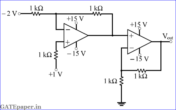
2.
In the circuit shown below, the
OP-AMPs are ideal. Then Vout in volts is
a. 4
b. 6
c. 8
d. 10
2014
1.
In the low pass filter shown in the
figure, for a cutoff frequency of 5 KHz, the value of R2 (in KΩ) is ……..
Answer: 3.18
2.
In the voltage regulator circuit
shown in the figure, the Op-Amp is ideal. The BJT has VBE = 0.7
volts, and β
= 100, and the zener voltage is 4.7 volts. For a regulated output of 9 volts,
the value of R (in Ω)
is ……..
Answer: 1090
3.
In the circuit shown, the Op-Amp has
finite input resistance, infinite voltage gain and zero input offset voltage.
The output voltage Vout is …….
a. – I2(R1 + R2)
b. I2R2
c. I1R2
d. – I1(R1 + R2)
Answer: C
4.
In the differential amplifier shown
in the figure, the magnitude of the common mode and differential mode gains are
Acm and Ad, respectively. If the resistance RE
is increased, then
a. Acm increases
b. Common mode rejection ratio increases
c. Ad increases
d. Common mode rejection ratio decreases
Answer: B
5.
Assuming that the Op-Amp in the
circuit is ideal, then the output voltage is
Answer: D
6.
The circuit represents
a. A band pass filter
b. A voltage controlled oscillator
c. An Amplitude modulator
d. A monostable multivibrator
Answer: D
1.
In
the circuit shown, assume OP-AMP is ideal then the 3 dB cut off frequency (in
Hz) is __________
Answer: 159.15
2.
In
the circuit shown, assume that the OP-AMP is ideal. If the gain (Vo/Vin)
is –12 , then the value of R (in kΩ) is _________________
Answer: 1 Kohm
3.
In
the circuit shown, assume that the OP-AMP is ideal. The bridge output voltage Vo
(in mV) for δ = 0.05 is _______________
Answer: 250
4.
The
circuit shown in the figure has an ideal OP-AMP. The oscillation frequency and
the condition to sustain the oscillations respectively are ________________
Answer: D
5.
In
the circuit shown, I1 = 80 mA and I2 = 4 mA. Transistors
T1 and T2 are identical. Assume that thermal voltage is
26 mV at 27oC. At 50oC, the value of voltage V12
= V1 – V2 (in mV) is _______________
Answer: 83.4
6.
In
the circuit shown, Vo = VOA for switch SW in position A
and Vo = VOB for switch SW in position B. Assume that the
OP-AMP is ideal. The value of VOB/VOA is ______________
Answer: 1.5
7. In the bistable
circuit shown, the ideal OP-AMP ahs saturation levels of ± 5 volts. The value
of R1 (in kΩ) that gives a hysteresis width of 500 mV is
_________________
Answer: 1 Kohm
8. Assuming that
the OP-AMP in the circuit shown is ideal, the output voltage Vo (inn
volts) is __________
Answer: 12
9. For the voltage
regulator circuit shown,the input voltage (Vin) is 20 V ± 20% and
the regulated output voltage (Vout) is 10 volts. Assume the OP-AMP
is ideal. For a load RL drawing 200 mA, the maximum power
dissipation in Q1 (in Watts) is _________________
Answer: 2.85