
1987
1.
The configuration of cascode
amplifier is
a.
CE – CE
b.
CE – CB
c.
CC – CB
d.
CC – CC
Answer: B
1988
1.
Each transistor in the Darlington
pair shown below has hFE = 100. The overall hFE of the
composite transistor, neglecting the leakage currents is

a.
10000
b.
10001
c.
10100
d.
10200
Answer: C
2.
The amplifier circuit shown below
uses a composite transistor of a MOSFET and BIPOLAR in cascade. All
capacitances are large. gm of the MOSFET is 2 mA/V, and hfe
of the BIPOLAR is 99. The overall Transconductance gm of the
composite transistor is

a.
198 mA/V
b.
9.9 mA/V
c.
4.95 mA/V
d.
1.98 mA/V
Answer: D
1992
1.
The Two Port Darlington impedance
booster of figure uses identical transistors (hie = 1 KΩ, hfe = 100, hre = hoe =
0).

Calculate
the Z – parameters of the network. Use relevant approximations.
Answer: Z11 = Z21 = 10.3 MΩ and Z12 = Z22 = 1 KΩ
Solution: https://www.youtube.com/watch?v=lCOs9-FKM4I
1995
1. In the amplifier circuit shown, determine the value of R
such that Q2 is biased at VCE2 = 7.5 volts. Assume Q1
and Q2 to be identical with VBE = 0.7 volts.

Also
determine the small signal input impedance of Q1 and Q2,
if both of them have β
= 200. Use VT = 26 mV.
1996
1.
A Darlington stage is shown in the
figure. If the Transconductance of Q1 is gm1 and Q2
is gm2, then the overall Transconductance gmc ≡ [icc/vbec] is given
by

a.
gm1
b.
0.5 gm1
c.
gm2
d.
0.5 gm2
Answer: C
1997
1.
A cascode
amplifier stage is equivalent to
a.
A common emitter stage followed by a
common base stage
b.
A common base stage followed by an
emitter follower
c.
An emitter follower stage followed
by a common base stage
d.
A common base stage followed by a
common emitter stage
Answer: A
Solution : https://www.youtube.com/watch?v=SPCOV6Ty37Y
1998
1.
A multistage amplifier has a low
pass response with three real poles at s = - ω1, - ω2 and -ω3. The
approximate overall bandwidth B of the amplifier will be given by

Answer: B
Solution : https://www.youtube.com/watch?v=6qJInA6Xyu0
2002
1.
Three identical RC coupled
transistor amplifiers are cascaded. If each of the amplifiers has a frequency
response as shown in the figure, the overall frequency response is as given in
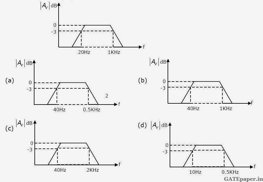
Answer: A
Solution : https://www.youtube.com/watch?v=EtdsNaauT8g
2. Below figure shown is a 2 – stage amplifier.

The
transistors Q1 and Q2 are identical with current gain β = 100, further βDC =
βac = β. The zener diode Dz has a break down region and
its dynamic resistance rz is zero. The capacitors C1 and
C2 are large and provide negligible impedance at signal frequencies.
a. Identify
the configuration in each of the amplifier stages. (i.e. whether CE, CC or CB)
b. Determine
the quiescent quantities of IC1 and VC1.
c. Determine
an expression for the voltage gain Vo/Vs and determine
its value. (Assume VBE = 0.7 volts, ro = ∞ and thermal
voltage VT = 25mV)
Answer:
Solution:
2003
1. Three identical amplifiers with each one having a voltage
gain of 50, input resistance of 1 KΩ and output resistance of 250 Ω are cascaded. The open circuit voltage gain of the combined
amplifier is
a.
49 dB
b.
51 dB
c.
98 dB
d.
102 dB
Answer: C
Solution : https://www.youtube.com/watch?v=Mv94EuUazrQ
2005
1.
The cascode amplifier is a
multistage configuration of
a.
CC – CB
b.
CE – CB
c.
CB – CC
d.
CE – CC
Answer: B
Solution : https://www.youtube.com/watch?v=srt3MdOny5g
2010
1.
In the silicon BJT circuit shown
below, assume that the emitter area of transistor Q1 is half that of
transistor Q2. The value of current Io is approximately

a.
0.5 mA
b.
2 mA
c.
9.3 mA
d.
15 mA
Answer: B
Solution : https://www.youtube.com/watch?v=jWdra3gmHK0
2014
1.
A cascade connection of two voltage
amplifiers A1 and A2 is shown in the figure. The open loop gain Avo,
input resistance Rin, and output resistance Ro for A1 and
A2 are as follows:
A1 : Avo = 10,
Rin = 10 KΩ, Ro = 1 KΩ
A2 : Avo = 5,
Rin = 5 KΩ, Ro
= 200 Ω
The approximate overall voltage gain Vout / Vin
is …………….
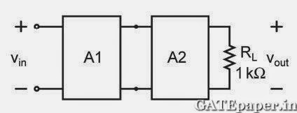
Answer: 35
No comments:
Post a Comment