
1988
1.
The quiescent collector current IC,
of a transistor is increased by changing resistances. As a result
a.
gm will not be effected
b.
gm will decrease
c.
gm will increase
d.
gm will increase or
decrease depending upon bias stability
Answer: C
2.
The amplifier circuit shown below
uses a composite transistor of a MOSFET and BIPOLAR in cascade. All
capacitances are large. gm of the MOSFET is 2 mA/V, and hfe
of the BIPOLAR is 99. The overall Transconductance gm of the
composite transistor is

a.
198 mA/V
b.
9.9 mA/V
c.
4.95 mA/V
d.
1.98 mA/V
Answer: D
3.
The transistor in the amplifier
shown below has following parameters: hfe = 100, hie = 2
kΩ,
hre = 0, hoe = 0.05 mhos. All capacitors are very large.
The output impedance is

a.
20 kΩ
b.
16 kΩ
c.
5 kΩ
d.
4 kΩ
Answer: D
1990
1.
Which of the following statements
are correct for biasing transistor amplifier configurations?
a.
CB amplifier has low input impedance
and a low current gain
b.
CC amplifier has low output
impedance and a low current gain
c.
CE amplifier has very poor voltage
gain but has very high input impedance
d.
The current gain of CB amplifier is
higher than the current gain of CC amplifier
Answer: A
1991
1.
In figure, both transistors are
identical and have a high value of β. Take the DC base emitter voltage drop as 0.7 volts and
KT/q = 25 mV. The small signal low frequency voltage gain (Vo/Vi)
is equal to __________

Answer: 120
2.
Two non-inverting amplifiers, one
having a unity gain and the other having a gain of 20 are made using identical
operational amplifiers. As compared to unity gain amplifier, the amplifier with
gain 20 has
a.
Less negative feedback
b.
Greater negative feedback
c.
Less bandwidth
d.
None of the above
Answer: A & C
1993
1.
For the amplifier circuit of figure,
the transistor has a β
of 800. The mid band voltage gain Vo/V1 of the circuit
will be

a.
0
b.
< 1
c.
= 1
d.
800
Answer: B
Solution : https://www.youtube.com/watch?v=vhDfv4p7h1g
1994
1.
A common emitter transistor
amplifier has a collector current of 1.0 mA when its base current is 25 µA at room temperature. Its input resistance is approximately
equal to _______
Answer: 1kΩ
1995
1.
An RC coupled amplifier is assumed
to have a single pole low frequency transfer function. The maximum lower cutoff
frequency allowed for the amplifier to pass 50 Hz square wave with no more than
10% tilt is ______________
Answer: 150 Hz
2.
Match the following:
a)
CC amplifier 1) provides voltage gain but no current gain
b)
CE amplifier 2) provides current gain but no voltage gain
c)
CB amplifier 3) provides neither voltage nor power gain
4) provides neither
current nor power gain
5) provides both voltage
and current gain
Answer: a-2, b-3, c-1
1996
1.
In the circuit shown, ‘N’ is a
finite gain amplifier with a gain of K, large input impedance and very low
output impedance. The input impedance of the feedback amplifier with the
feedback impedance Z connected as shown will be ______________

Answer: D
2. A common emitter amplifier with an external capacitors CC
connected across the base and the collector of the transistor is shown. Given gm
= 5 mA/V, rπ
= 20 kΩ,
Cπ
= 1.5 pF and Cµ
= 0.5 pF.

a.
Determine the ac small signal mid
band voltage gain, Vo/Vs.
b.
Determine the upper cutoff frequency
fH of the amplifier.
Answer: (a) -33.33 (b) 18.326 KHz
1997
1.
In the BJT amplifier shown in
figure, the transistor is based in the forward active region. Putting a
capacitor across RE will
a.
Decrease the voltage gain and
decrease the input impedance
b.
Increase the voltage gain and
decrease the input impedance
c.
decrease the voltage gain and
increase the input impedance
d.
Increase the voltage gain and
increase the input impedance
Answer: B
Solution : https://www.youtube.com/watch?v=dyVSC2Y1uGI
2. The transistor in the circuit shown is so biased (dc biasing network is not shown) that the dc collector current, IC = 1 mA and VCC = 5 volts. The network components have following values: RC = 2 kΩ, RS = 1.4 kΩ and RE = 100 Ω. The transistor has β = 100 and a base spreading resistance, rbb’ = 100Ω. Assume VT = 25 mV.

Evaluate
small signal voltage gain AVS at a frequency of 10 kHz, and input
resistance Ri for two cases:
a. CE, the bypass capacitor across RE is
25 µF
b. The bypass capacitor CE is removed leaving RE
unbypassed
Answer: (a) -50, 2.5 kΩ (b) -14.2, 12.6 KΩ
Solution : https://www.youtube.com/watch?v=RoUrqP0JRF4
1998
1. In the circuit shown, determine the resistance Ro
seen by the output terminals. Ignore the effect of R1 and R2.

1999
1.
An amplifier is assumed to have a
single pole high frequency transfer function. The rise time of its output
response to a step function input is 35 nsec. The upper -3 dB frequency (in
MHz) for the amplifier to a sinusoidal input is approximately at
a.
4.55
b.
10
c.
20
d.
28.6
Answer: B
Solution : https://www.youtube.com/watch?v=-8aPpRbUUjI
2. A bipolar junction transistor amplifier is shown below.
Assume that the current source Ibias is ideal, and the transistor
has very large β,
rb = 0 and r0 -> ∞.

Determine
the ac small signal mid band voltage gain (Vo / Vs),
input resistance (Ri) and output resistance (Ro) of the
circuit. Assume VT = 26 mV.
2000
1.
Introducing a resistor in the
emitter of a CE amplifier stabilizes the dc operating point against variations
in
a.
Only the temperature
b.
Only the β of the transistor
c.
Both temperature and β
d.
None of the above
Answer: C
Solution : https://www.youtube.com/watch?v=Hj4RgZDwBwk
2. For the amplifier circuit shown, IC = 1.3 mA, RC
= 2 kΩ,
RE = 500 Ω,
VT = 26 mV, β
= 100, VCC = 15 volts, VS = 0.01 sin(ωt) volts and Cb = Ce = 10 µF.

a.
What is the small signal voltage
gain, Vo/VS
b.
What is the approximate voltage gain
if Ce is removed?
c.
What will be the output Vo, if Cb
is short circuited?
3. Below figure shown is a common base amplifier.

a.
Write expressions for the time
constants associated with the capacitances Cb and Cs.
b.
What is the approximate lower cutoff
frequency of the amplifier?
Answer:
τCb = 2π(re + RE//RS),
τCs = 2π(re//RE +RS)CS,
fCb = 1/τCb , fCs = 1/ τCs ,
overall fL = Max{ fCb , fCs }
τCb = 2π(re + RE//RS),
τCs = 2π(re//RE +RS)CS,
fCb = 1/τCb , fCs = 1/ τCs ,
overall fL = Max{ fCb , fCs }
Solution : https://www.youtube.com/watch?v=wTtlORiy598
2001
1.
The current gain of a BJT is
a.
gmro
b.
gm / ro
c.
gmrπ
d.
gm / rπ
Answer: C
Solution : https://www.youtube.com/watch?v=NQcoEO5xLYk
2. An emitter follower amplifier is shown below, where Zi
is the impedance looking into the base of the transistor and Zo is
the impedance looking into the emitter of the transistor.

a.
Draw the small signal equivalent
circuit of the amplifier.
b.
Obtain an expression for Zi.
c.
Obtain an expression for Zo.
d.
Determine Zi and Zo,
if a capacitor C is connected across R1.
Answer:
(b) Zi = rπ + (1 + β)RL
(c) Zo = (RS + rπ)/(1 + β)
(d) Zi = rπ + (1 + β)ZL and Zo = (RS + rπ)/(1 + β)
Solution: https://www.youtube.com/watch?v=UH5_EioJdxU
2003
1.
Choose the correct match of input
resistance of various amplifier configurations shown below:
Configuration
Input
resistance
CB : Common Base
LO : Low
CC : Common Collector
MO : Moderate
CE : Common Emitter
HI : High
a.
CB – LO, CC – MO, CE – HI
b.
CB – LO, CC – HI, CE – MO
c.
CB – MO, CC – HI, CE – LO
d.
CB – HI, CC – LO, CE
– MO
Answer: B
Solution : https://www.youtube.com/watch?v=KEJiSEq93hw
2004
1.
A bipolar transistor is operating in
the active region with a collector current of 1 mA. Assuming that the β of the transistor is 100 and the thermal voltage (VT)
is 25 mV. The Transconductance (gm) and the input resistance (rπ) of the transistor in the common emitter configuration are
a.
gm = 25 mA/V and rπ = 15.625 KΩ
b.
gm = 40 mA/V and rπ = 4.0 KΩ
c.
gm = 25 mA/V and rπ = 2.5 KΩ
d.
gm = 40 mA/V and rπ = 2.5 KΩ
Answer: D
Solution : https://www.youtube.com/watch?v=cK0KRkqCWVw
2006
Common
Data for Questions (1, 2 and 3):
In the transistor amplifier circuit shown in the figure
below, the transistor has the following parameters: βDC = 60, VBE
= 0.7 volts, hie -> ∞, hoe -> ∞. The
capacitance CC can be assumed to be infinite.

1.
Under the DC conditions, the collector to
emitter voltage drop is
a.
4.8 volts
b.
5.3 volts
c.
6.0 volts
d.
6.6 volts
Answer: C
2.
If βDC is increased by 10%, the collector to emitter
voltage drop
a.
Increases by less than or equal to
10%
b.
Decreases by less than or equal to
10%
c.
Increases by more than 10%
d.
Decreases by more than 10%
Answer: B
3.
The small signal gain of the
amplifier Vo/Vs is
a.
– 10
b.
– 5.3
c.
+ 5.3
d.
+ 10
2008
Statement
for Linked Answer Question:
In the following transistor circuit, VBE = 0.7
volts, re = 25 mV/IE, β and all the capacitances are very large.

1. The value of DC current IE is
a.
1 mA
b.
2 mA
c.
5 mA
d.
10 mA
Answer: A
2.
The mid-band voltage gain of the
amplifier is approximately
a.
– 180
b.
– 120
c.
– 90
d.
– 60
Answer: D
Solution : https://www.youtube.com/watch?v=eX0es1gFdW4
2009
1.
A small signal source Vi(t) =
Acos20t + Bsin106t is applied to a transistor amplifier as shown
below. The transistor has β
= 150 and hie = 3 KΩ. Which expression best approximate Vo(t).

a.
Vo(t) = - 1500 (Acos20t +
Bsin106t)
b.
Vo(t) = - 150 (Acos20t +
Bsin106t)
c.
Vo(t) = - 1500 (Bsin106t)
d.
Vo(t) = - 150 (Bsin106t)
Answer: D
Solution : https://www.youtube.com/watch?v=C-1mKYDJhY4
2010
1.
The amplifier circuit shown below
uses a silicon transistor. The capacitors CC and CE can
be assumed to be short at signal frequency and effect of output resistance ro
can be ignored. If CE is disconnected from the circuit, which one of
the following statements is TRUE.

a.
The input resistance Ri
increases and magnitude of voltage gain AV decreases
b.
The input resistance Ri
decreases and magnitude of voltage gain AV increases
c.
The input resistance Ri
decreases and magnitude of voltage gain AV decreases
d.
The input resistance Ri
increases and magnitude of voltage gain AV increases
Answer: A
Solution : https://www.youtube.com/watch?v=E48_Y4CYKIU
Common
Data Questions:
Consider the common emitter amplifier shown below with the
following circuit parameters.
β = 100, gm = 0.3861 A/V, ro = 259 Ω, RS = 1 KΩ, RB = 93 KΩ, RC = 250 Ω, RL = 1 KΩ, C1 = ∞ and C2 = 4.7 µF.

2.
The resistance seen by the source VS
is
a.
258 Ω
b.
1258 Ω
c.
93 KΩ
d.
∞
Answer: B
3.
The lower cutoff frequency due to C2
is
a.
33.9 Hz
b.
27.1 Hz
c.
13.6 Hz
d.
16.9 Hz
Answer: B
Solution : https://www.youtube.com/watch?v=FdpAV2BR7Fc
2011
1.
In the circuit shown below,
capacitors C1 and C2 are very large and are shorts at
the input frequency . vi is a
small signal input. The gain magnitude |V0/Vi| at 10 M
rad/sec is

a.
Maximum
b.
Minimum
c.
Unity
d.
Zero
Answer: A
Solution : https://www.youtube.com/watch?v=OL8a4oM3MhM
2012
1.
The current ib through
the base of a silicon NPN transistor is 1+0.1cos (10000πt) mA. At 300oK, the rπ in the small signal model of the transistor is ________ (in
Ohms).

a.
250
b.
27.5
c.
25
d.
22.5
Answer: C
Solution : https://www.youtube.com/watch?v=LvH15dfxkVE
2.
The impedance looking into nodes 1
and 2 in the given circuit is________ (in Ohms).

a.
50
b.
100
c.
5K
d.
10.1 K
Answer: A
Solution : https://www.youtube.com/watch?v=M7px_ck8xa4
3.
The voltage gain Av, of
the circuit shown below is

a.
|Av| ≡ 200
b.
|Av| ≡ 100
c.
|Av| ≡ 20
d.
|Av| ≡ 10
Answer: D
Solution : https://www.youtube.com/watch?v=u07jd8J7Sfw
2014
1.
A BJT is biased in forward active
mode. Assume VBE = 0.7 volts, KT/q = 25 mV and reverse saturation
current IS = 10-13 Amp. The Transconductance of the BJT
(in mA/volt) is…..
Answer: 5785
Solution : https://www.youtube.com/watch?v=nAh0aTdVp84
2.
For the amplifier shown in the
figure, the BJT parameters are VBE = 0.7 volts, β = 200, and thermal voltage VT = 25 mV. The
voltage gain (vo/vi) of the amplifier is ……..

Answer: -232
Solution : https://www.youtube.com/watch?v=YTAqzayIguA
3.
If the emitter resistance in a
common emitter voltage amplifier is not bypassed, it will
a.
Reduce both the voltage gain and the
input impedance
b.
Reduce the voltage gain and increase
the input impedance
c.
Increase the voltage gain and reduce
the input impedance
d.
Increase both the voltage gain and
the input impedance
Answer: B
Solution : https://www.youtube.com/watch?v=4YjclPDw5lM
4.
Consider two BJTs biased at the same
collector current with area A1 = 0.2 µm x 0.2 µm
and A2 = 300 µm
x 300 µm.
assuming that all other device parameters are identical, KT/q = 26 mV, the
intrinsic carrier concentration is 1 x 1010 cm-3, and q =
1.6 x 10⁻¹⁹C, the difference between the base emitter voltages (in
mV) of the two BJTs (i.e. VBE1 – VBE2) is …………….
Answer: 380
5.
A BJT in a common base configuration
is used to amplify a signal received by a 50Ω antenna. Assume KT/q = 25 mV, the value of collector bias
current (in mA) required to match the input impedance of the amplifier to the
impedance of the antenna is ………..
Answer: 0.5
Solution : https://www.youtube.com/watch?v=HBjqJb91WbE
6.
Consider the common collector amplifier
in the figure (bias circuitry ensures that the transistor operates in forward
active region, but has been omitted for simplicity). Let IC be the
collector current, VBE be the base emitter voltage and VT
be the thermal voltage. Also, gm and ro are the small
signal Transconductance and output resistance of the transistor, respectively.
Which one of the following conditions ensures a nearly constant small signal
voltage gain for a wide range of values of RE?
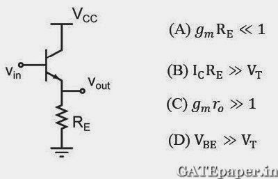
Answer: B
2015
1. Consider the bode plot shown in figure. Assume that all the poles and zeros are real valued. The value of fH – fL (in Hz) is _____________

1. Consider the bode plot shown in figure. Assume that all the poles and zeros are real valued. The value of fH – fL (in Hz) is _____________
Answer: 8970
Solution: https://www.youtube.com/watch?v=R95T4ztuNQo
Solution: https://www.youtube.com/watch?v=R95T4ztuNQo
2. In the ac equivalent
circuit shown, the two BJTs are biased in active region and have identical parameters
with β>>1. The open circuit small signal voltage gain is
approximately is _________________

Answer: 1
Solution: https://www.youtube.com/watch?v=BPjWJXi5TZ4
Solution: https://www.youtube.com/watch?v=BPjWJXi5TZ4
shit
ReplyDeleteMore not available
ReplyDelete