GATE 1995 ECE Analog Circuits (Analog Electronics) - Video Solutions

1. A change in the value of the emitter resistance, RE, in a differential amplifier
a. affects the difference mode gain Ad
b. affects the common mode gain Ac
c. affects both Ad and Ac
d. does not affect both Ad and Ac.
Answer: B
Solution : https://www.youtube.com/watch?v=czxo7TomyPc


2. To obtain very high input and output impedance in a feedback amplifier, the topology mostly used is
a. Voltage Series
b. Current Series
c. Voltage Shunt
d. Current Shunt
Answer: B
Solution : https://www.youtube.com/watch?v=xfuv73dQbBA


3. In the given circuit, if the voltage V+ and V_ are to amplified by the same factor, the value of R should be _________

Answer:33 kΩ
Solution : https://www.youtube.com/watch?v=iyaRnnLhxNI


4. An NPN transistor under forward active mode of operation is biased at Ic = 1 mA, and has a total emitter base capacitance CK of 12 pF, and the base transit time τF of 260 psec. Under this condition, the depletion capacitance of the emitter base junction is _____________
Answer: 2 pF
Solution : https://www.youtube.com/watch?v=faoewgwLY0o


5. An RC coupled amplifier is assumed to have a single pole low frequency transfer function. The maximum lower cutoff frequency allowed for the amplifier to pass 50 Hz square wave with no more than 10% tilt is ______________
Answer: 150 Hz
Solution : https://www.youtube.com/watch?v=Y7Pez6ot4bQ


6. An OP-AMP is used as a zero crossing detector. If the maximum output available from the OP-AMP is ±12 volts peak to peak, and the slew rate of the OP-AMP is 12 V/µsec, then the maximum frequency of the input signal that can be applied without causing a reduction in the peak to peak output is _____________
Answer: 1.59 KHz
Solution : https://www.youtube.com/watch?v=xMs3KYXPxeQ


7. A power amplifier delivers 50W output at 50% efficiency. The ambient temperature is 25oC. If the maximum allowable junction temperature is 150oC, then the maximum thermal resistance øjc that can be tolerated is __________
Answer:2.5 oC/W
Solution : https://www.youtube.com/watch?v=aOpeF9Z9hlQ


8. An amplifier has an open loop gain of 100, and its lower and upper cutoff frequency of 100 Hz and 100 kHz respectively. A feedback network with a feedback factor of 0.99 is connected to the amplifier. The new lower and upper cutoff frequencies are at __________ and ________
Answer: 1 Hz and 10 MHz
Solution : https://www.youtube.com/watch?v=R7lcv_H47gE


9. Match the following:
a) CC amplifier 1) provides voltage gain but no current gain
b) CE amplifier 2) provides current gain but no voltage gain
c) CB amplifier 3) provides neither voltage nor power gain
4) provides neither current nor power gain
5) provides both voltage and current gain
Answer: a-2, b-3, c-1
Solution : https://www.youtube.com/watch?v=6I1uAhJPB10

10. Sketch the output as a function of the input voltage (for negative values) for circuit shown below. Assume ideal operational amplifier and diode forward voltage drop as zero.

Answer:(a) 0 Volts (b) -Vin
Solution: https://www.youtube.com/watch?v=ulb3JFwnZDs


11. The waveform input to the sweep generator circuit shown in figure, is a square wave of period 2 msec and amplitude varying between 0 and 12 volts.

a. Draw the waveform Vo(t), in relation to the input
b. Specify Vo(t) determine the voltage levels and the time constants involved.

Solution: https://www.youtube.com/watch?v=MqLJPriVFVw


12. In the JFET circuit shown, assume that R1//R2 = 1 MΩ and the total stray capacitance at the output to be 20 pF.

Determine the upper cutoff frequency of the amplifier.
Answer: 3.18 MHz
Solution: https://www.youtube.com/watch?v=joc09FhNQI8


13. Show that the circuit shown in figure is double integrator. In other words, prove that the transfer gain is given by Vo(s)/Vs(s) = 1/(SCR)2, assume ideal operational amplifier.

Solution: https://www.youtube.com/watch?v=kIlrli8NFJ0


14. In the amplifier circuit shown, determine the value of R such that Q2 is biased at VCE2 = 7.5 volts. Assume Q1 and Q2 to be identical with VBE = 0.7 volts.

Also determine the small signal input impedance of Q1 and Q2, if both of them have β = 200. Use VT = 26 mV.
Answer: R= 2.72 kΩ, Ri1 < 1 kΩ, Ri2 = 5.65 kΩ
Solution: https://www.youtube.com/watch?v=CiBKrmFWjC8

GATE 1996 ECE Analog Circuits (Analog Electronics) - Video Solutions

1. In the circuit of the given figure, assume that the diodes are ideal and the meter is an average indicating ammeter. The ammeter will read ________

Answer: D
Solution : https://www.youtube.com/watch?v=RrGtXsrXhr0


2. The circuit shown in the figure is that of

a. A Non-inverting amplifier
b. An Inverting amplifier
c. An Oscillator
d. A Schmitt trigger
Answer: D
Solution : https://www.youtube.com/watch?v=CUm0AtZGCJA


3. In the circuit shown, ‘N’ is a finite gain amplifier with a gain of K, large input impedance and very low output impedance. The input impedance of the feedback amplifier with the feedback impedance Z connected as shown will be ______________

Answer: D
Solution : https://www.youtube.com/watch?v=4ISLXf0p9WM


4. A Darlington stage is shown in the figure. If the Transconductance of Q1 is gm1 and Q2 is gm2, then the overall Transconductance gmc ≡ [icc/vbec] is given by

a. gm1
b. 0.5 gm1
c. gm2
d. 0.5 gm2
Answer: C
Solution : https://www.youtube.com/watch?v=UHqoUnpLM7I


5. Value of R in the oscillator circuit shown in the given figure, so chosen that it just oscillates at an angular frequency of ω. The value of ω and the required value of R will respectively are

a. 105 rad/sec, 2 x 10⁴
b. 2 x 10⁴ rad/sec, 2 x 10⁴
c. 2 x 10⁴ rad/sec, 105
d. 105 rad/sec, 105
Answer: A
Solution : https://www.youtube.com/watch?v=cf3HdmbWYks


6. A common emitter amplifier with an external capacitors CC connected across the base and the collector of the transistor is shown. Given gm = 5 mA/V, rπ = 20 kΩ, Cπ = 1.5 pF and Cµ = 0.5 pF.

a. Determine the ac small signal mid band voltage gain, Vo/Vs.
b. Determine the upper cutoff frequency fH of the amplifier.
Answer: (a) -33.33 (b) 18.326 KHz
Solution: https://www.youtube.com/watch?v=15wQMy8qg8A


7. A resistively loaded and resistively biased differential amplifier circuit is shown. Neglect base current and assume matched transistors with VA -> ∞ and β = 100. Use VT = 26 mV, VBE(on) = 0.7 volts and VCE(sat) = 0.1 volts.

a. Determine the values of RC and RE to meet the following specifications: double ended differential mode gain = 500, CMRR = 500 and differential mode input resistance of 2 MΩ.
b. Determine the minimum values of VCC and VEE such that the transistors remain in the forward active region under zero signal condition. Assume that the DC common mode input is zero.
Answer: (a) 5 MΩ, 2.5 MΩ (b) 12.6 Volts, -13.83 Volts
Solution: https://www.youtube.com/watch?v=9zaM7i-wdmI


8. Assuming ideal operational amplifiers, show that the circuit shown simulates in inductor i.e. show that Vi(S)/Ii(S) is inductive and write the expression for the effective inductance.

Answer: Leff = C.R2
Solution: https://www.youtube.com/watch?v=PJTRIK_taJA


GATE Pratice Questions on "Digital Circuits - 1"


1.       Identify the operation performed by the following circuit, where A and B are 4 bit inputs.


2.       Find the modulus of the following asynchronous counter circuit


3.       Find the output expression for the following circuit.


4.       Identify the operation performed by given sequential circuit.


5.       Minimize the following circuit and realize the circuit using only minimum number of 2 input NAND gates


6.       Find the combinational logic expression realized by the given MUX.


7.       Find the relation between CLKA and CLK and also between CLKB and CLK.


8.       Find the output for different values of inputs as shown for the given JK flip flop.


9.       Determine the resulting serial data that appear on the output ‘Q’. Assume there is one clock pulse for each bit time, Q is initially zero and preset and clear inputs are HIGH initially. Rightmost bits are applied first.


10.   Find the modulus of the following synchronous counter.


11.   Find the relation between clock frequency and output frequency at Q.


12.   An AB flip-flop is shown for all possible input combinations. Write the truth table of the flip-flop.


GATE practice Problems on PN junction (Diode) Set - 2


1.       An ideal silicon PN junction has a reverse saturation current of 0.1 µA at a temperature of 125oC. Find the dynamic resistance at 105oC when the diode is forward biased with 0.8 volts.


2.       An ideal germanium diode at room temperature has a static resistance of 4.57 Ω at a point, where the current flowing is 43.8 mA. Find the dynamic resistance for a forward bias of 0.1 volt.


3.       For an alloy silicon PN junction with NA << ND, calculate depletion layer capacitance (CT), if the resistivity of P-material is 4 Ω-cm, the barrier height Vo = 0.3 volts, applied reverse voltage is 4 volts and the cross sectional area is circular of 50 mills in diameter.


4.       Find the resistivity of the P-type material in a silicon PN junction, where cross sectional area is circular and of 40 mils in diameter and the transition capacitance is 61 pF. The given barrier height is 0.35 volts and the applied reverse voltage is 5 volts.


5.       For a silicon P+N junction with ND = 1015 atoms per cm3 and the built in potential of 0.5 volts. Find the transition capacitance per square mil, if the applied reverse voltage is 10 volts.


6.       The transition capacitance of an abrupt PN junction is 10 pF at 4 volts. Find the decrease in capacitance for a 0.5 volts increase in bias.


7.       For a silicon PN junction with NA = ND = 1021 atoms per m3 and ni = 9.8 x 10¹⁵ atoms per m3. Calculate transition capacitance, if the area is 1 mm2 and the junction is reverse biased with 10 volts.


8.       Find static and dynamic resistances of a PN junction germanium diode for an applied forward bias of 0.2 volts, if the temperature is 300oK and reverse saturation current of 1 µA.


9.       Find the Diffusion capacitance of a silicon diode with NA >> ND, when carrying a current of 1 mA. Assume diffusion length of holes i 0.026 cm.


10.   The zero barrier height of an alloy silicon PN+ junction is 0.6 volts and acceptor concentration is 5 x 10¹⁶ atoms per cm3. Find space charge capacitance for an applied reverse voltage of 5.6 volts, if the cross sectional area is 1 mm2.


11.   For a silicon P+N junction, find the current flowing through the junction, if the diffusion length is 2.6 µm and diffusion capacitance is 1 nF.


12.   Calculate the barrier capacitance of a germanium PN junction, whose area is 0.5 mm X 0.5 mm and space charge thickness, is 3 x 10⁻⁴ cm.


13.   In the given figure, the V-I characteristics of the diode is given as I = 0.2(V – 1)1/2 for V ≥ 1 else zero. Find the current ‘I’ indicated.


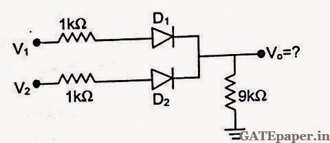
14.   For the circuit shown, assume the drop across conducting diode is 0.7 volts. Find Vo if V1 = 10 volts and V2 = 5 volts.


15.   For the circuit shown, Find the voltage drop across diode D1, if V1 = 5 volts and V2 = 0 volts. Assume ideal diodes.


16.   For the circuit shown, assume that the silicon diode requires a minimum current of 1 mA to be above the knee of its I-V characteristic.
a.       What should be the value of R to establish 5 mA in the circuit?
b.      With the value of R calculated, what is the minimum value of voltage E, such that the diode current is above the knee point.


17.   For the circuit shown, assume that the silicon diode is biased above its knee and has a bulk resistance of 0.1 Ω. Find the total current in and total voltage across the diode. Sketch the current versus time.


18.   Determine which diodes are forward biased and which are reverse biased in each of the configurations shown in figure.


19.   Determine which diodes are forward biased and which are reverse biased in the circuits shown. Assume a 0.7 volts drop across each forward biased diode, determine the output voltage also.


20.   A diode conducts a current of 440 nA form cathode to anode, when the reverse biasing voltage across it is 8 volts. What is the diode resistance?


21.   For the circuit shown, the current I is 34.28 mA. What is the voltage drop across the diode and also find its DC resistance?


22.   For the circuit shown, assume that the voltage drop across a forward biased silicon diode is 0.7 volts and that across a germanium diode is 0.3 volts.
a.       If D1 and D2 are both silicon diodes, find the current I in the circuit.
b.      Find the current I in the circuit, if D1 is silicon and D2 is germanium.


23.   In the circuit shown below, assume the diode is germanium. Find the percent error caused by neglecting the voltage drop across the diode, when calculating the current I in the circuit. Assume voltage drop across forward biased germanium diode is 0.3 volts.


24.   In the circuit shown, the diode has 0.65 volts drop across it.
a.       Find the DC current in the diode
b.      Find ac resistance of the diode at room temperature
c.       Find total current in and total voltage across the diode
d.      What are the minimum and maximum values of current flowing through the diode?


25.   In the circuit shown, the voltage source is a square wave whose output alternates between + 2.5 volts and – 2.5 volts. Find the peak voltage across and current through the resistor, if the diode is germanium and R = 330 Ω.


26.   Determine which of the following diodes are forward biased and which are reverse biased.


27.   Determine which of the following diodes are forward biased and which are reverse biased.


28.   In the circuit shown, the inputs A and B can be either 0 volts or +10 volts. Each diode is silicon and has resistance 400 Ω when it is forward biased. Find Vo for all four possible combinations of A and B.


29.   In circuit shown, the inputs A, B and C can be either +10 volts or –5 volts. Each diode is silicon and has a resistance of 1200Ω when it is forward biased. Find Vo, when
a.       A = B = C = -5 volts
b.      A = B = C = +10 volts
c.       A = C = -5 volts and B = +10 volts
d.      A = B = +10 volts and C = -5 volts


30.   In the circuit shown, the inputs A and B can be either 0 volts or -5 volts. Assuming that the forward voltage of the diode is 0.7 volts, find Vo for all possible combinations of A and B.


Post Your Feedback (or) Doubts here.......

Name

Email *

Message *