
1.
An ideal silicon PN junction has a reverse
saturation current of 0.1 µA at a temperature of 125oC. Find the
dynamic resistance at 105oC when the diode is forward biased with
0.8 volts.
2.
An ideal germanium diode at room temperature has
a static resistance of 4.57 Ω at a point, where the current flowing is 43.8 mA.
Find the dynamic resistance for a forward bias of 0.1 volt.
3.
For an alloy silicon PN junction with NA
<< ND, calculate depletion layer capacitance (CT),
if the resistivity of P-material is 4 Ω-cm, the barrier height Vo =
0.3 volts, applied reverse voltage is 4 volts and the cross sectional area is
circular of 50 mills in diameter.
4.
Find the resistivity of the P-type material in a
silicon PN junction, where cross sectional area is circular and of 40 mils in
diameter and the transition capacitance is 61 pF. The given barrier height is
0.35 volts and the applied reverse voltage is 5 volts.
5.
For a silicon P+N junction with ND
= 1015 atoms per cm3 and the built in potential of 0.5
volts. Find the transition capacitance per square mil, if the applied reverse
voltage is 10 volts.
6.
The transition capacitance of an abrupt PN
junction is 10 pF at 4 volts. Find the decrease in capacitance for a 0.5 volts
increase in bias.
7.
For a silicon PN junction with NA = ND
= 1021 atoms per m3 and ni = 9.8 x 10¹⁵
atoms per m3. Calculate transition capacitance, if the area is 1 mm2
and the junction is reverse biased with 10 volts.
8.
Find static and dynamic resistances of a PN
junction germanium diode for an applied forward bias of 0.2 volts, if the
temperature is 300oK and reverse saturation current of 1 µA.
9.
Find the Diffusion capacitance of a silicon
diode with NA >> ND, when carrying a current of 1
mA. Assume diffusion length of holes i 0.026 cm.
10.
The zero barrier height of an alloy silicon PN+
junction is 0.6 volts and acceptor concentration is 5 x 10¹⁶ atoms
per cm3. Find space charge capacitance for an applied reverse
voltage of 5.6 volts, if the cross sectional area is 1 mm2.
11.
For a silicon P+N junction, find the
current flowing through the junction, if the diffusion length is 2.6 µm and
diffusion capacitance is 1 nF.
12.
Calculate the barrier capacitance of a germanium
PN junction, whose area is 0.5 mm X 0.5 mm and space charge thickness, is 3 x
10-4 cm.
13.
In the given figure, the V-I characteristics of
the diode is given as I = 0.2(V – 1)1/2 for V ≥ 1 else zero. Find
the current ‘I’ indicated.

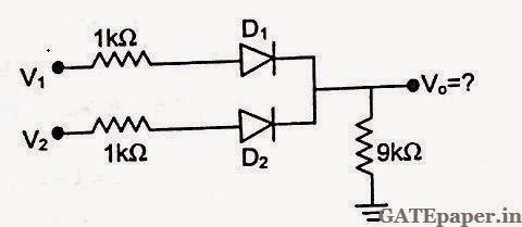
14.
For the circuit shown, assume the drop across conducting
diode is 0.7 volts. Find Vo if V1 = 10 volts and V2
= 5 volts.
15.
For the circuit shown, Find the voltage drop
across diode D1, if V1 = 5 volts and V2 = 0
volts. Assume ideal diodes.

16.
For the circuit shown, assume that the silicon
diode requires a minimum current of 1 mA to be above the knee of its I-V
characteristic.
a.
What should be the value of R to establish 5 mA
in the circuit?
b.
With the value of R calculated, what is the
minimum value of voltage E, such that the diode current is above the knee point.

17.
For the circuit shown, assume that the silicon
diode is biased above its knee and has a bulk resistance of 0.1 Ω. Find the
total current in and total voltage across the diode. Sketch the current versus
time.

18.
Determine which diodes are forward biased and
which are reverse biased in each of the configurations shown in figure.

19.
Determine which diodes are forward biased and
which are reverse biased in the circuits shown. Assume a 0.7 volts drop across
each forward biased diode, determine the output voltage also.

20.
A diode conducts a current of 440 nA form
cathode to anode, when the reverse biasing voltage across it is 8 volts. What
is the diode resistance?
21.
For the circuit shown, the current I is 34.28
mA. What is the voltage drop across the diode and also find its DC resistance?

22.
For the circuit shown, assume that the voltage
drop across a forward biased silicon diode is 0.7 volts and that across a
germanium diode is 0.3 volts.
a.
If D1 and D2 are both
silicon diodes, find the current I in the circuit.
b.
Find the current I in the circuit, if D1
is silicon and D2 is germanium.

23.
In the circuit shown below, assume the diode is
germanium. Find the percent error caused by neglecting the voltage drop across
the diode, when calculating the current I in the circuit. Assume voltage drop
across forward biased germanium diode is 0.3 volts.

24.
In the circuit shown, the diode has 0.65 volts
drop across it.
a.
Find the DC current in the diode
b.
Find ac resistance of the diode at room
temperature
c.
Find total current in and total voltage across
the diode
d.
What are the minimum and maximum values of
current flowing through the diode?

25.
In the circuit shown, the voltage source is a
square wave whose output alternates between + 2.5 volts and – 2.5 volts. Find
the peak voltage across and current through the resistor, if the diode is
germanium and R = 330 Ω.

26.
Determine which of the following diodes are
forward biased and which are reverse biased.

27.
Determine which of the following diodes are
forward biased and which are reverse biased.

28.
In the circuit shown, the inputs A and B can be
either 0 volts or +10 volts. Each diode is silicon and has resistance 400 Ω
when it is forward biased. Find Vo for all four possible
combinations of A and B.

29.
In circuit shown, the inputs A, B and C can be either
+10 volts or –5 volts. Each diode is silicon and has a resistance of 1200Ω when
it is forward biased. Find Vo, when
a.
A = B = C = -5 volts
b.
A = B = C = +10 volts
c.
A = C = -5 volts and B = +10 volts
d.
A = B = +10 volts and C = -5 volts

30.
In the circuit shown, the inputs A and B can be
either 0 volts or -5 volts. Assuming that the forward voltage of the diode is
0.7 volts, find Vo for all possible combinations of A and B.
No comments:
Post a Comment