Showing posts with label Practice Problems EDC. Show all posts

GATE Practice Problems on JFET (Junction Field Effect Transistor)

1.       An N-channel JFET has VP = -4 volts and IDSS = 10 mA.
a.       Find the minimum VDS for the device to operate in pinch-off, when VGS = -2 volts.
b.      Find the drain current for VGS = -2 volts, when VDS is 3 volts and 5 volts.

2.       The JFET in the circuit has VP = - 3 volts, IDSS = 9 mA. Find the values of all resistors so that VG = 5 volts, ID = 4 mA and VD = 11 volts. Design for 0.05 mA in the voltage divider.


3.       An N-channel silicon JFET has a donor concentration of 2 x 10²¹ /m3 and a channel width of 4 µm.
a.       Find the pinch off voltage, VP
b.      Find the saturation voltage, VDSsat, if VGS is  – 2 volts.


4.       The Q-point of a JFET in a source self-bias arrangement is chosen at VGS = - 1.5 volts and ID = 5 mA. Find the value of the resistance RS.


5.       An N-channel JFET has IDSS = 12 mA and the Transconductance of 4mA/V when VGS = 0 volts.
a.       Find the pinch off voltage, VP
b.      Find the drain current when VGS = - 2 volts.


6.       An N-channel JFET has pinch off voltage of – 4.5 volts and IDSS = 9 mA.
a.       At what value of VGS in the pinch off region will ID equal to 3 mA?
b.      What is the value of VDS(sat), when ID = 3 mA?


7.       For the given JFET, IDSS = 10 mA and VP = - 4 volts. Find the quiescent values of ID and VDS, when VGS = - 1.5 volts. Assume that JFET is biased in pinch off region.


8.       For the circuit shown, find the Q-point, when VGS = - 3 volts.


9.       For the P-channel JFET shown, find the Q-point if IDSS = 18 mA and VP = 5 volts.


10.   An N-channel JFET has IDSS = 16 mA and VP = - 6 volts. Calculate the drain current and VDS(sat) when VGS = - 4 volts.


11.   A P-channel JFET has a pinch off voltage of 8 volts. At what value of VGS does VDS(sat) = - 3 volts?


12.   An N-channel JFET has pinch off voltage of – 5.8 volts and IDSS = 15 mA. Find the value of ID when VGS is 0 volts, - 2 volts and – 6.5 volts.


13.   An N-channel JFET having a pinch off voltage of – 3.5 volts has a saturation current of 2.3 mA when VGS = - 1 volt. What is its saturation current when VGS = 0 volts and -2 volts.


14.   A P-channel JFET has a pinch off voltage of 6 volts and IDSS = 18 mA. At what value of VGS in the pinch off region will ID equal 6 mA? What is the value of VDS at pinch off point?


15.   The JFET shown has IDSS = 14 mA and VP = - 5 volts. Determine the Q-point for 
a.       VGS = - 3.6 volts
b.      VGS = - 3 volts
c.       VGS = - 1.7 volts


16.   Find the Q-point of the JFET shown, if IDSS = 6 mA and VP = - 3 volts.


17.   Determine the values of ID,VGS and VDS for the JFET shown, if IDSS = 25 mA and VP = 8 volts.


18.   Determine the values of ID, VGS and VDS of the JFET circuit shown, if IDSS = 2.42 mA and VP = - 4 volts.


19.   Find the values of ID and VDS of the N-channel JFET shown, if IDSS = 12 mA and VP = - 5 volts.


GATE practice Problems on PN junction (Diode) Set - 2


1.       An ideal silicon PN junction has a reverse saturation current of 0.1 µA at a temperature of 125oC. Find the dynamic resistance at 105oC when the diode is forward biased with 0.8 volts.


2.       An ideal germanium diode at room temperature has a static resistance of 4.57 Ω at a point, where the current flowing is 43.8 mA. Find the dynamic resistance for a forward bias of 0.1 volt.


3.       For an alloy silicon PN junction with NA << ND, calculate depletion layer capacitance (CT), if the resistivity of P-material is 4 Ω-cm, the barrier height Vo = 0.3 volts, applied reverse voltage is 4 volts and the cross sectional area is circular of 50 mills in diameter.


4.       Find the resistivity of the P-type material in a silicon PN junction, where cross sectional area is circular and of 40 mils in diameter and the transition capacitance is 61 pF. The given barrier height is 0.35 volts and the applied reverse voltage is 5 volts.


5.       For a silicon P+N junction with ND = 1015 atoms per cm3 and the built in potential of 0.5 volts. Find the transition capacitance per square mil, if the applied reverse voltage is 10 volts.


6.       The transition capacitance of an abrupt PN junction is 10 pF at 4 volts. Find the decrease in capacitance for a 0.5 volts increase in bias.


7.       For a silicon PN junction with NA = ND = 1021 atoms per m3 and ni = 9.8 x 10¹⁵ atoms per m3. Calculate transition capacitance, if the area is 1 mm2 and the junction is reverse biased with 10 volts.


8.       Find static and dynamic resistances of a PN junction germanium diode for an applied forward bias of 0.2 volts, if the temperature is 300oK and reverse saturation current of 1 µA.


9.       Find the Diffusion capacitance of a silicon diode with NA >> ND, when carrying a current of 1 mA. Assume diffusion length of holes i 0.026 cm.


10.   The zero barrier height of an alloy silicon PN+ junction is 0.6 volts and acceptor concentration is 5 x 10¹⁶ atoms per cm3. Find space charge capacitance for an applied reverse voltage of 5.6 volts, if the cross sectional area is 1 mm2.


11.   For a silicon P+N junction, find the current flowing through the junction, if the diffusion length is 2.6 µm and diffusion capacitance is 1 nF.


12.   Calculate the barrier capacitance of a germanium PN junction, whose area is 0.5 mm X 0.5 mm and space charge thickness, is 3 x 10⁻⁴ cm.


13.   In the given figure, the V-I characteristics of the diode is given as I = 0.2(V – 1)1/2 for V ≥ 1 else zero. Find the current ‘I’ indicated.


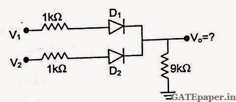
14.   For the circuit shown, assume the drop across conducting diode is 0.7 volts. Find Vo if V1 = 10 volts and V2 = 5 volts.


15.   For the circuit shown, Find the voltage drop across diode D1, if V1 = 5 volts and V2 = 0 volts. Assume ideal diodes.


16.   For the circuit shown, assume that the silicon diode requires a minimum current of 1 mA to be above the knee of its I-V characteristic.
a.       What should be the value of R to establish 5 mA in the circuit?
b.      With the value of R calculated, what is the minimum value of voltage E, such that the diode current is above the knee point.


17.   For the circuit shown, assume that the silicon diode is biased above its knee and has a bulk resistance of 0.1 Ω. Find the total current in and total voltage across the diode. Sketch the current versus time.


18.   Determine which diodes are forward biased and which are reverse biased in each of the configurations shown in figure.


19.   Determine which diodes are forward biased and which are reverse biased in the circuits shown. Assume a 0.7 volts drop across each forward biased diode, determine the output voltage also.


20.   A diode conducts a current of 440 nA form cathode to anode, when the reverse biasing voltage across it is 8 volts. What is the diode resistance?


21.   For the circuit shown, the current I is 34.28 mA. What is the voltage drop across the diode and also find its DC resistance?


22.   For the circuit shown, assume that the voltage drop across a forward biased silicon diode is 0.7 volts and that across a germanium diode is 0.3 volts.
a.       If D1 and D2 are both silicon diodes, find the current I in the circuit.
b.      Find the current I in the circuit, if D1 is silicon and D2 is germanium.


23.   In the circuit shown below, assume the diode is germanium. Find the percent error caused by neglecting the voltage drop across the diode, when calculating the current I in the circuit. Assume voltage drop across forward biased germanium diode is 0.3 volts.


24.   In the circuit shown, the diode has 0.65 volts drop across it.
a.       Find the DC current in the diode
b.      Find ac resistance of the diode at room temperature
c.       Find total current in and total voltage across the diode
d.      What are the minimum and maximum values of current flowing through the diode?


25.   In the circuit shown, the voltage source is a square wave whose output alternates between + 2.5 volts and – 2.5 volts. Find the peak voltage across and current through the resistor, if the diode is germanium and R = 330 Ω.


26.   Determine which of the following diodes are forward biased and which are reverse biased.


27.   Determine which of the following diodes are forward biased and which are reverse biased.


28.   In the circuit shown, the inputs A and B can be either 0 volts or +10 volts. Each diode is silicon and has resistance 400 Ω when it is forward biased. Find Vo for all four possible combinations of A and B.


29.   In circuit shown, the inputs A, B and C can be either +10 volts or –5 volts. Each diode is silicon and has a resistance of 1200Ω when it is forward biased. Find Vo, when
a.       A = B = C = -5 volts
b.      A = B = C = +10 volts
c.       A = C = -5 volts and B = +10 volts
d.      A = B = +10 volts and C = -5 volts


30.   In the circuit shown, the inputs A and B can be either 0 volts or -5 volts. Assuming that the forward voltage of the diode is 0.7 volts, find Vo for all possible combinations of A and B.


GATE practice Problems on PN junction (Diode) Set - 1


1.       Calculate built in potential of a germanium PN junction at 300oK, if P-side is doped with 5 x 10¹⁶ acceptors/cm3 and N-side with 5 x 10¹⁴ donors/cm3.


2.       The resistivites of the two sides of an abrupt silicon PN junction are 9.6 Ω-cm on P-side and 100 Ω-cm on N-side. Find contact potential at room temperature.


3.       For what voltage, will the reverse current in a PN junction silicon diode reach 95% of its saturation value at room temperature?


4.       What is the ratio of currents for a forward bias of 0.1 volt to the current for the same magnitude of reverse bias of silicon PN junction at room temperature?


5.       If the reverse saturation current in a silicon PN junction is 1 nA. Find the applied voltage for a forward current of 0.5 µA?


6.       A silicon diode at room temperature conducts 5 mA at 0.7 volts. If the voltage increases to 0.8 volts, find the diode current.


7.       What is the change in voltage at 300oK for a tenfold increase in current for a silicon diode operating in the conducting region?


8.       For a silicon diode operating under conducting region at room temperature, if the voltage is increased by 0.24 volts, then the current flowing through it increases by _______ number of times.


9.       Calculate the factor by which the reverse saturation current of a germanium diode is multiplied, when the temperature is increased from 20 to 100oC.


10.   What increase in temperature would result in a reverse saturation current, which is 50 times its value at room temperature?


11.   A silicon diode operates at a forward voltage of 0.7 volts. Calculate the factor by which the current will be multiplied, when the temperature is decreased from 25oC to – 55oC.


12.   For a silicon P+N junction, ND = 1015 atoms/cm3 and the built in potential of 0.5 volts. If the applied reverse voltage is 10 volts, find the value of electric field at the junction.


13.   Calculate the width of depletion region of a PN junction under open circuit, when doped equally on both sides with 1021 atoms/m3. Assume built in potential of 0.2 volts and εr = 10.


14.   Find the magnitude of the electric field at the center of depletion region of silicon PN junction with NA = ND = 1021 atoms per m3 and built in potential of 0.6 volts.


15.   If the reverse saturation current of diode is 30 nA, then voltage across the diode is ___________________


16.   The zero voltage barrier height of an alloy silicon PN+ junction is 0.6 volts, given NA = 5 x 10¹⁶ atoms/cm3. Calculate the width of depletion layer for an applied reverse voltage of 5.6 volts.


17.   The zero voltage barrier height of an alloy silicon P+N junction is 0.6 volts, given ND = 5 x 10¹⁶ per cm3. Calculate the width of depletion layer for an applied forward voltage of 0.5 volts.


18.   A silicon PN junction is formed from P material doped with 1022 acceptors/m3 and N material doped with 1.2 x 10²¹ donors/m3. Find the thermal voltage and barrier voltage at 27oC.


19.   A silicon diode has a saturation current of 0.1 pA at 20oC. Find its current when it is forward biased by 0.55 volts. Find the current in the same diode when the temperature rises to 100oC.


20.   A silicon PN junction is formed from N material doped with  2.5 x 10²¹ donors/m3 and P material doped to have the same impurity density. Assume ni = 1.5 x 10¹⁶ /m3 and is temperature independent.
a.       Find thermal voltage and barrier voltage at 40oC.
b.      To what temperature would the junction have to be raised (in oC) in order that the thermal voltage be 30 mV? What would be the barrier voltage at that temperature?


21.   A silicon PN junction has a saturation current of 1.8 x 10⁻¹⁴ A. Assuming that η=1 and the temperature is 27oC.
a.       Find the current in the junction when the forward biasing voltage is 0.6 volts .
b.      Repeat (a) when forward biasing voltage is 0.65 volts.


22.   The forward current in a PN junction is 1.5 mA at 27oC. If Io = 2.4 x 10⁻¹⁴ A and η = 1. What is the forward biasing voltage across the junction?


23.   The forward current in a PN junction is 22 mA, when the forward biasing voltage is 0.64 volts. If the thermal voltage is 26 mV and η = 1, find the reverse saturation current?


24.   A bar of silicon is doped so that one side (side A) has 1.85 x 10²²  electrons/m3 and the other side (side B) has 2.66 x 10¹⁰ electrons/m3. If the bar is to be used as a junction diode, which side should be the anode and which side is cathode?


25.   The reverse breakdown voltage of a certain diode is 150 volts and its reverse saturation current is 0.1 pA. What is the current in the diode, when the reverse bias voltage is 149.95 volts? Assume constant n = 2.


26.   For a certain diode, a reverse current of 9.3 nA was measured when the reverse voltage across the diode was 349.99 volts. If the breakdown voltage is 350 volts and reverse saturation current is 0.1 pA, find the value of the constant ‘n’?


27.   A diode has its maximum power dissipation rating as 0.1 watts and its reverse breakdown voltage as 200 volts. What maximum reverse current does it sustain at breakdown without damage?


28.   A diode has a reverse breakdown voltage of 100 volts and a saturation current of 0.05 pA. How much power does it dissipate when the reverse voltage is 99.99 volts? Assume constant n = 2.5.


29.   A diode has a reverse saturation current of 45 pA at a temperature of 373oK. What is the approximate value of Io at 273oK?


30.   When the voltage across a forward biased diode at T = 10oC is 0.621 volts and the current is 4.3 mA. If the current is held constant, what is the voltage at T = 40oC and T= - 30oC.

Post Your Feedback (or) Doubts here.......

Name

Email *

Message *