Showing posts with label GATE 2015. Show all posts

GATE 2015 ECE Network Theory - Complete Video Solutions with Answers


2015

1. In the network shown in the figure, all resistors are identical with R = 300 Ω. The resistance Rab (in Ω) of the network is __________________


Answer: 100
Solution :       https://www.youtube.com/watch?v=R2Lsmws8L2U


2. In the circuit shown, at resonance, the amplitude of the sinusoidal voltage (in volts) across the capacitor is ____________________


Answer: 25
Solution :         https://www.youtube.com/watch?v=YZq-lDiqadg


3. In the circuit shown, the switch SW is thrown from position A to position B at time t=0. The energy (in µJ) taken from the 3 volts source to charge the 0.1 µF capacitor from 0 volts to 3 volts is


a) 0.3
b) 0.45
c) 0.9
d) 3


Answer: C
Solution :       https://www.youtube.com/watch?v=ZbFt7Lkclp8


4. In the given circuit, the values of V1 and V2 (in volts) respectively are


a) 5, 25
b) 10, 30
c) 15, 35
d) 0, 20


Answer: A
Solution :       https://www.youtube.com/watch?v=0YY9dEZPVUI


5. In the circuit shown, switch SW is closed at t =0. Assuming zero initial conditions, the value of Vc(t) (in volts) at t = 1 sec is __________________


Answer: 2.528
Solution :       https://www.youtube.com/watch?v=_hcH81bC-cg


6. In the given circuit, the maximum power (in Watts) that can be transferred to the load RL is _______


Answer: 1.649
Solution :    https://www.youtube.com/watch?v=Hr4AS712hRM   


7. In the circuit shown, the average value of the voltage Vab (in volts) in steady state condition is _________


Answer: 5
Solution :       https://www.youtube.com/watch?v=ysVaNyiOZtw


8. The 2 – port Admittance matrix of the circuit shown is given by____________


Answer: A
Solution :       https://www.youtube.com/watch?v=jQZIEyucrjU


9. The voltage (Vc) across the capacitor (in volts) in the network shown is ______________


Answer: 100
Solution :     https://www.youtube.com/watch?v=BiEeuX6a218    


10. An LC tank circuit consists of an ideal capacitor C connected in parallel with a coil of inductance L having an internal resistance R. The resonant frequency of the tank circuit is


Answer: B
Solution :       https://www.youtube.com/watch?v=Y331K9dgrPs


11. In the circuit shown, the initial voltages across the capacitors C1 and C2 are 1 volt and 3 volts respectively. The switch is closed at time t = 0. The total energy dissipated (in Joules) in the resistor R until steady state is reached, is _______________


Answer: 3
Solution :       https://www.youtube.com/watch?v=wj9gkVjceEk


12. In the circuit shown, the Norton equivalent resistance (in Ω) across terminals a and b is ________


Answer: 1.33
Solution :       https://www.youtube.com/watch?v=w8z1zeVVm1c


13. At High frequencies, the peak output voltage Vo (in volts) is __________


Answer: 0.5
Solution:           https://www.youtube.com/watch?v=_O4UfZGA87c              


14. For the current shown in the figure, the Thevenin equivalent voltage (in volts) across terminals a and b is _______________


Answer: 10
Solution :       https://www.youtube.com/watch?v=JNhFCs7jQiM


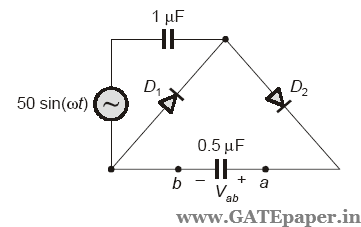
15. In the circuit shown, assume that diodes D1 and D2 are ideal. In the steady state condition, the average voltage Vab (in volts) across 0.5 µF capacitor is ____________


Answer: 100
Solution :       https://www.youtube.com/watch?v=2ZfO7mplk4g


16. In the circuit shown, the voltage Vx (in volts) is __________


Answer: 8
Solution :       https://www.youtube.com/watch?v=nfrqvps0ojs


17. In the circuit shown, assume that the diodes D1 and D2 are ideal. The average voltage Vab (in volts) across terminals a and b is _____________


Answer: 5
Solution :        https://www.youtube.com/watch?v=nK21y4c_m0Q 


18. In the circuit shown, the current I flowing through the 50 Ω resistor will be zero, if the value of the capacitor C (in µF) is __________________


Answer: 20
Solution :       https://www.youtube.com/watch?v=ZSJIgQWJiKU


19. The ABCD parameters of the following 2 – port network are


Answer: B
Solution :       https://www.youtube.com/watch?v=iIjMzXmILXk


Control Systems - GATE Paper 2015 ECE Video Solutions


2015

1. The polar plot of the transfer function G(s) = 10(s+1)/(s+10) for 0 < ω < will be in the
a) first quadrant
b) second quadrant
c) third quadrant
d) fourth quadrant

Answer:A


2. A unity negative feedback system has the open loop transfer function
the value of the gain K (>0) at which the root locus crosses the imaginary axis is __________________

Answer:12


3. A lead compensator network includes a parallel combination fo R and C in the feed-forward path. If the transfer function of the compensator is GC(s) = (s+2)/(s+4) , the value of RC is ___________

Answer:0.5


4. A plant transfer function is given as
When the plant operates in a unity feedback configuration, the condition for the stability of the closed loop system is
a) KP > KI/2 > 0
b) 2KI > KP > 0
c) 2KI < KP
d) 2KI > KP

Answer:A


5. The open loop transfer function of a unity feedback configuration is given as
The value of a gain K( >0 ) for which -1+j2 lies on the root locus is _________.

Answer:25.54


6. A unity negative feedback system has an open loop transfer function G(s) = K / S(S+10), the gain K for the system to have a damping ratio of 0.25 is _____________

Answer:400


7. For the signal flow graph shown in the figure, the value of C(s)/R(s) is

Answer:B


8. By performing cascading and/or summing/differencing operations using transfer function blocks G1(s) and G2(s), one CANNOT realize a transfer function of the form


Answer:B


9. The transfer function of a mass-spring-damper system is given by
the frequency response data for the system are given in the following table.
The unit step response of the system approaches a steady state value of _____________


Answer:0.4


10. The state variable representation of a system is given as
The response y(t) is
a) sin (t)
b) 1 et
c) 1 – cos (t)
d) 0


Answer:D


11. The output of a standard second order system for a unit step input is given as
The transfer function of the system is

Answer:D


12. Consider the differential equation dx/dt = 10 – 0.2x with initial condition x(0) = 1. The response x(t) for t > 0 is
a) 2 – e-0.2t
b) 2 – e0.2t
c) 50 – 49e-0.2t
d) 50 – 49e0.2t


Answer:C


13. The transfer function of a first order controller is given as Gc(s) = K(s+a) / (s+b), where K, a and b are positive real numbers. The condition for this controller to act as a phase lead compensator is
a) a < b
b) a > b
c) K < ab
d) K > ab

Answer:A


14. Consider the Bode plot shown in figure.
Assume that all the poles and zeros are real valued. The value of fHfL (in Hertz) is ____________________

Answer:8970


15. The phase margin (in degrees ) of the system G(s) = 10 /s(s+10) is _____________


Answer:83


16. The characteristic equation of an LTI system is given by F(s) = s5 + 2s4 + 3s3 + 6s2 – 4s – 8 = 0. The number of roots that lie strictly in the left half S – plane is __________.

Answer:2


17. A network is described by the state model as
then the transfer function H(s) = (Y(s)/U(s)) is


Answer:A


18. For the system shown in figure, s = - 2.75 lies on the root locus if K is ____________


Answer:0.3


19. The position control of a DC servo-motor is given in the figure. The values of the parameters are KT = 1 N-mA, Ra = 1 ohm, La = 0.1 H, J = 5 kg-m2, B = 1 N-m/(rad/sec) and Kb = 1 volt/(rad/sec). The steady state position response(in radians) due to unit impulse disturbance torque Td is _______.

Answer:0.5


GATE 2015 Question papers with complete Answer Key for all braches released by IIT Kanpur


GATE 2015 : Answer Key

Date / Day Answer Key
Session No. Time Paper Codes (For Answer Key)
31st January 2015
(Saturday)
1 9:00 Hrs - 12:00 Hrs
[FN Session]
AG, AR, BT, CH, CY, EC, EY, XE, XL
2 14:00 Hrs - 17:00 Hrs
[AN Session]
EC, ME,
1st February 2015
(Sunday)
3 9:00 Hrs - 12:00 Hrs
[FN Session]
EC, ME,
4 14:00 Hrs - 17:00 Hrs
[AN Session]
AE, GG, IN, MA, ME, MN, MT, PH, PI, TF
7th February 2015
(Saturday
)
5 9:00 Hrs - 12:00 Hrs
[FN Session]
CS, EE
6 14:00 Hrs - 17:00 Hrs
[AN Session]
CS, EE
8th February 2015
(Sunday)
7 9:00 Hrs - 12:00 Hrs
[FN Session]
CE, CS
8 14:00 Hrs - 17:00 Hrs
[AN Session]
CE

GATE 2015 ECE Digital Circuits (Digital Electronics) - Video Solutions

GATE 2015 ECE – Questions on Digital Circuits with Solutions
1. The circuit shown consists of JK flip flops, each with an active LOW asynchronous reset. The counter corresponding to this circuit is ___________

a. Mod – 5 binary UP counter
b. Mod – 6 binary DOWN counter
c. Mod – 5 binary DOWN counter
d. Mod – 6 binary UP counter
Answer:A
Solution: https://www.youtube.com/watch?v=nSMpwmgMQNc


2. In the circuit shown, D1, D2 and D3 are ideal and inputs E1, E2 and E3 are 0 volts for logic’0’ and 10 volts for logic ‘1’. What logic gate does the circuit represent?

a. 3 input OR gate
b. 3 input NOR gate
c. 3 input AND gate
d. 3 input XOR gate
Answer:C
Solution: https://www.youtube.com/watch?v=lA-egB6GmAo


3. A universal gate can implement any Boolean function by connecting sufficient number of them appropriately. Three gates are shown.

Which one of the following statements is TRUE?
a. Gate 1 is universal gate
b. Gate 2 is universal gate
c. Gate 3 is universal gate
d. None of the gates shown is universal gate
Answer:D
Solution: https://www.youtube.com/watch?v=hJ2MSI9840A


4. A three bit pseudo random number generator is shown. Initially the value of output Y = Y2Y1Y0 is set to 111. The value of output Y after three clock cycles is _________

a. 000
b. 001
c. 010
d. 100
Answer:D
Solution: https://www.youtube.com/watch?v=yeKpE3yuXAk


5. An SR latch is implemented using TTL gates as shown in the figure. The set and reset pulse inputs are provided using the push button switches. It is observed that the circuit fails to work as desired. The SR latch can be made functional by changing

a. NOR gates to NAND gates
b. Inverters to Buffers
c. NOR gates to NAND gates and inverters to buffers
d. 5 volts to ground
Answer:D
Solution: https://www.youtube.com/watch?v=tmpeSu-gXZQ


6. Consider a four bit Digital to Analog converter. The analog value corresponding to a digital signals of values 0000 and 0001 are 0 volts and 0.0625 volts respectively. The analog value (in volts) corresponding to the digital signal 1111 is ______________
Answer:0.9375
Solution: https://www.youtube.com/watch?v=m5TBDdQ7Uwg


7. In a 8085 microprocessor, the shift registers which store the result of an addition and the overflow bit are respectively
a. B and F
b. A and F
c. H and F
d. A and C
Answer:B
Solution: https://www.youtube.com/watch?v=MSKB0ExFE9g


8. A 16 KB memory array is designed as a square with an aspect ratio of one (number of rows is equal to the number of columns). The minimum number of address lines needed for the row decoder is ______________
Answer:7
Solution: https://www.youtube.com/watch?v=Dmj_YCiX7uE


9. A 3 input majority gate is defined by the logic function M(a,b,c) = ab + bc + ca. Which one of the following gate is represented by the function M(M’(a,b,c),M(a,b,c’),c)?
a. 3 input NAND gate
b. 3 input XOR gate
c. 3 input NOR gate
d. 3 input XNOR gate
Answer:B
Solution: https://www.youtube.com/watch?v=e4wDfHig2cc


10. The Boolean expression F(x,y,z) = x’yz’+xy’z’+xyz’+xyz converted into canonical product of sum (POS) form is ___________

Answer:A
Solution: https://www.youtube.com/watch?v=wFow-s9t4Kw


11. All the logic gates shown in the figure have a propagation delay of 20 ns. Let A=C=0 and B=1 until time t = 0. At t = 0, all the inputs flip (i.e. A=C=1 and B=0) and remain in that state. For t>0, output z=1 for a duration (in 20 ns) of____________

Answer:40
Solution: https://www.youtube.com/watch?v=KywM3DmY8i0


12. A Mod-N counter using a synchronous binary UP counter with asynchronous clear input is shown in the figure. The value of N is_______________

Answer:7
Solution: https://www.youtube.com/watch?v=Cn3ylcDYyug


13. In the figure shown, the output Y is required to be Y = AB+C’D’. The gates G1 and G2 must be _____

a. NOR, OR
b. OR, NAND
c. NAND, OR
d. AND, NAND
Answer:A
Solution: https://www.youtube.com/watch?v=sjtdMcvFqDU


14. In an 8085 microprocessor, which one of the following instructions changes the content of the accumulator?
a. MOV B,M
b. PCHL
c. RNZ
d. SBI BEH .
Answer:D
Solution: https://www.youtube.com/watch?v=_VVI3E46Nag


15. A function of Boolean variables X,Y and Z is expressed in terms of the min-terms as F(X,Y,Z) = ∑m(1,2,5,6,7). Which one of the product of sums given below is equal to the given function?

Answer:B
Solution: https://www.youtube.com/watch?v=HPihAxUd608


16. The figure shows a binary counter with synchronous clear input. With the decoding logic shown, the counter works as a _______________

a. Mod – 2 counter
b. Mod – 4 counter
c. Mod – 5 counter
d. Mod – 6 counter
Answer:C
Solution: https://www.youtube.com/watch?v=UQ_-E6h7XpE


17. Problem on Design of 1 to 8 De-multiplexer using two 2 to 4 decoders with extra logic gates.

Answer:D
Solution: https://www.youtube.com/watch?v=FYl68C2-fmo

Post Your Feedback (or) Doubts here.......

Name

Email *

Message *