Showing posts with label GATE 2009. Show all posts

GATE 2009 ECE Network Theory - Complete Video Solutions with Answers

2009


1. A fully charged mobile phone with a 12 volts battery is good for a 10 min talk time.
Assume that, during the talk time, the battery delivers a constant current of 2 Amp and its voltage drops linearly from 12 volts to 10 volts as shown in the figure. How much energy does the battery deliver during this talk-time?
a) 220 J
b) 12 kJ
c) 13.2 kJ
d) 14.4 kJ

Answer: C
Solution:     https://www.youtube.com/watch?v=GV1gFYMN_wc


2. In the interconnection of ideal sources shown in figure, it is known that the 60 volts source is absorbing power. Which of the following can be the value of the current source I?
a) 10 A
b) 13 A
c) 15 A
d) 18 A

Answer: A
Solution:     https://www.youtube.com/watch?v=2mwLjmGEWzo


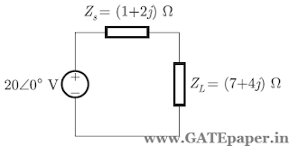
3. An AC source of RMS voltage 20 volts with internal impedance Zi = (1+2j) Ω feeds a load of impedance ZL = (7+4j) Ω in the figure below. The reactive power consumed by the load is
a) 8 VAR
b) 16 VAR
c) 28 VAR
d) 32 VAR

Answer: B
Solution:      https://www.youtube.com/watch?v=w36Rox8j0KA


4. The switch in the circuit shown was on position 'a' for a long time, and is moved to position 'b' at time t=0. The current i(t) for t > 0 is given by

Answer: B
Solution:    https://www.youtube.com/watch?v=ptI9Yzy17OQ


5. In the circuit shown, what value of RL maximizes the power delivered to RL?
a) 2.4 Ω
b) 8/3 Ω
c) 4 Ω
d) 6 Ω

Answer: C
Solution:    https://www.youtube.com/watch?v=yqt0czRs6_I


6. The time domain behaviour of an RL circuit is represented as shown below. For an initial current of i(0) = Vo/R, the steady state value of the current is given by

Answer: A
Solution:     https://www.youtube.com/watch?v=VBFOXuUEuKE


GATE 2009 ECE Control Systems - Complete Video Solutions with Answers


2009

1. The magnitude plot of a rational transfer function G(s) with real coefficients is shown below. Which of the following compensator has such a magnitude plot?

a) Lead compensator
b) Lag compensator
c) PID compensator
d) Lead – Lag compensator

Answer:C


2. If the transfer function of the following circuit is Vo(s)/Vi(s) = 1/(2+sCR), then the value of the load resistor RL is

a) R/4
b) R/2
c) R
d) 2R

Answer:C


3. consider the system,
where p and q are arbitrary real numbers, which one of the following statements about the controllability of the system is TRUE?
a) the system is completely state controllable for any non zero values of p and q
b) only p=0 and q=0 result in controllability
c) the system is uncontrollable for all values of p and q
d) we cannot conclude about controllability from the given data

Answer:C


4. the feedback configuration and the pole-zero locations of G(s) = (s2 – 2s + 2)/(s2 + 2s +2), are shown below.
The root locus for negative values of k, i.e. for –∞ < k < 0, has break away/break in points and angle of departure at pole P (w.r.t. the positive real axis) equal to
a) ± √2 and 0o
b) ± √2 and 45o
c) ± √3 and 0o
d) ± √3 and 45o

Answer:B


5. The unit step response of an under damped second order system has steady state value of – 2. Which of the following transfer functions has these properties?


Answer:B


Common Data Questions: (6 & 7)
The Nyquist plot of a stable transfer function G(s) is shown in the figure. We are interested in the stability of the closed loop system in the feedback configuration shown.


6. Which of the following statements is TRUE?
a) G(s) is an all pass filter
b) G(s) has a zero in the right half plane
c) G(s) is the impedance of a passive network
d) G(s) is marginally stable

Answer:B

7. The gain and phase margin of G(s) for closed loop stability are
a) 6 dB and 180o
b) 3 dB and 180o
c) 6 dB and 90o
d) 3 dB and 90o

Answer:C


GATE 2009 ECE Video Solutions on Analog Circuits (Analog Electronics)

1. In the following Astable Multivibrator circuit, which properties of Vo(t) depend on R2 ?

a. Only the frequency
b. Only the amplitude
c. Both the amplitude and the frequency
d. Neither the amplitude nor the frequency
Answer:A
Solution: https://www.youtube.com/watch?v=CNrhstw1lQI


2. In the circuit shown below, the OP-AMP is ideal, the transistor has VBE = 0.6 volts and β = 150. Decide whether the feedback in the circuit is positive or negative and determine the voltage V at the output of the OP-AMP.

a. Positive feedback, V = 10 Volts
b. Positive feedback, V = 0 Volts
c. Negative feedback, V = 5 Volts
d. Negative feedback, V = 2 Volts
Answer:D
Solution: https://www.youtube.com/watch?v=H6FpEgr7ZYI


3. A small signal source Vi(t) = Acos20t + Bsin106t is applied to a transistor amplifier as shown below. The transistor has β = 150 and hie = 3 KΩ. Which expression best approximate Vo(t).

a. Vo(t) = - 1500 (Acos20t + Bsin106t)
b. Vo(t) = - 150 (Acos20t + Bsin106t)
c. Vo(t) = - 1500 (Bsin106t)
d. Vo(t) = - 150 (Bsin106t)
Answer:D
Solution: https://www.youtube.com/watch?v=C-1mKYDJhY4

GATE 2009 ECE Video Solution on Digital Circuits (Digital Electronics)

1. In a microprocessor, the service routine for a certain interrupt starts from a fixed location of memory which cannot be externally set, but the interrupt can be delayed or rejected. Such an interrupt is
a. non-maskable and non-vectored
b. maskable and non-vectored
c. non-maskable and vectored
d. maskable and vectored
Answer:D
Solution : https://www.youtube.com/watch?v=pJ-6A_o5-LU


2. If X = 1 in the given logic equation, then

a. Y = Z
b. Y = Z’
c. Z = 1
d. Z = 0
Answer:D
Solution : https://www.youtube.com/watch?v=qHzk5M1H6DU


3. What are the minimum number of 2 to 1 multiplexers required to generated a 2 input AND gate and a 2 input EX-OR gate?
a. 1 and 2
b. 1 and 3
c. 1 and 1
d. 2 and 2
Answer:A
Solution : https://www.youtube.com/watch?v=wixmXaKDQ5Q


4. Refer to the NAND and NOR latches shown in the figure. The inputs (P1, P2) for both the latches are first made (0, 1) and then, after a few seconds, made (1, 1). The corresponding stable outputs (Q1, Q2) are

Answer:C
Solution : https://www.youtube.com/watch?v=CmdmJ9qQjdk


5. What are the counting stages (Q1, Q2) for the counter shown in the figure below?


a. 11, 10, 00, 11, 10….
b. 01, 10, 11, 00, 01….
c. 00, 11, 01, 10, 00…..
d. 01, 10, 00, 01, 10…..
Answer:A
Solution : https://www.youtube.com/watch?v=marTcMTzg0Y


Statement for linked answer questions: 6 & 7
Two products are sold from a vending machine, which has two push buttons P1 and P2. When a button is pressed, the price of the corresponding product is displayed in a 7-segment display.
If no buttons are pressed, ‘0’ is displayed, signifying ‘Rs. 0’.
If only P1 is pressed, ‘2’ is displayed, signifying ‘Rs. 2’.
If only P2 is pressed, ‘5’ is displayed, signifying ‘Rs. 5’.
If both P1 and P2 are pressed, ‘E’ is displayed, signifying ‘Error’.
The names of the segments in the 7-segment display, and the glow of the display for ‘0’, ‘2’, ‘5’ and ‘E’ are shown below.

Consider
(i) Push button pressed / not pressed is equivalent to logic 1 / 0 respectively
(ii) A segment glowing / not glowing in the display is equivalent to logic 1 / 0 respectively
6. If segments a to g are considered as functions of P1 and P2, then which of the following is correct?

Answer:B

7. What are the minimum numbers of NOT gates and 2-inout OR gates required to design the logic of the driver for this 7-segment display?
a. 3 NOT and 4 OR
b. 2 NOT and 4 OR
c. 1 NOT and 3 OR
d. 2 NOT and 3 OR
Answer:D
Solution (6 & 7) : https://www.youtube.com/watch?v=njEr-LoSbw4

GATE 2009 ECE Video Solutions on EDC (Electronic Devices and Circuits)

1. In an N type silicon crystal at room temperature, which of the following can have a concentration of 4x1019 cm-3?
a. Silicon atoms
b. Holes
c. Dopant atoms
d. Valence electrons

Answer: C
Solution : https://www.youtube.com/watch?v=ck2TRWxTGGM


2. The full forms of the abbreviations TTL and CMOS in reference to logic families are
a. Triple Transistor Logic and Chip Metal Oxide semiconductor
b. Tristate Transistor Logic and Chip Metal Oxide semiconductor
c. Transistor Transistor Logic and Complementary Metal Oxide semiconductor
d. Tristate Transistor Logic and Complementary Metal Oxide semiconductor

Answer: C
Solution : https://www.youtube.com/watch?v=v-0BYB0NkMI

3. The ratio of the mobility to the diffusion coefficient in a semiconductor has the units
a. V-1
b. cm. V-1
c. V. cm-1
d. V.sec

Answer: A
Solution : https://www.youtube.com/watch?v=CbvKuwdmwPY


4. In the circuit below, the diode is ideal. The voltage V is given by

a. Min(Vi,1)
b. Max(Vi,1)
c. Min(-Vi,1)
d. Max(-Vi,1)

Answer: D
Solution : https://www.youtube.com/watch?v=yMHePwsPly0


5. Consider the following two statements about the internal conditions in an N channel MOSFET operating in the active region.
S1: the inversion charge decreases from source to drain
S2: the channel potential increases from source to drain
Which of the following is correct?
a. Both are TRUE
b. Both are FALSE
c. Both are TRUE, but S2 is not a reason for S1
d. Both are TRUE, and S2 is a reason for S1.

Answer: D
Solution : https://www.youtube.com/watch?v=qbq2JXNCe_Q


6. Common Data Question:
Consider a silicon PN junction at room temperature having the following parameters:
Doping on the N side = 1x1017 cm-3
Depletion width on N side = 0.1 µm
Depletion width on the P side = 1 µm
Intrinsic carrier concentration = 1.4x1010 cm-3
Thermal voltage = 26 mV
Permittivity of free space = 8.85x10⁻¹⁴ F/cm
Dielectric constant of silicon = 12

i. The built in potential of the junction is
a. 0.70 volts
b. 0.76 volts
c. 0.82 volts
d. Cannot be estimated from given data
Answer: B

ii. The peak electric field in the device is
a. 0.15 Mvolts/cm, directed from P region to N region
b. 0.15 Mvolts/cm, directed from N region to P region
c. 1.80 Mvolts/cm, directed from P region to N region
d. 1.80 Mvolts/cm, directed from N region to P region
Answer: B
Solution : https://www.youtube.com/watch?v=ZbOv57yZfQg


7. Linked Questions:
Consider the CMOS circuit shown, where the gate voltage VG of the N channel MOSFET is increased from zero, while the gate voltage of the P channel MOSFET is kept constant at 3 volts. Assume that, for both transistors, the magnitude of the threshold voltage is 1 volts and the product of the transconductance parameter and the (W/L) ratio i.e. the quantity µcox(W/L) is 1 mA/V2.

i. For small increase in VG beyond 1 volt, which of the following gives the correct description of the region of operation of each MOSFET?
a. Both are in saturation region
b. Both are in triode region
c. NMOS is in triode region and PMOS is in saturation region
d. NMOS is in saturation region and PMOS is in triode region
Answer: D

ii. Estimate the output voltage, Vo for VG = 1.5 volts. (Hint: use the appropriate current voltage equation for each MOSFET, based on the answer to above question)

Answer: C
Solution : https://www.youtube.com/watch?v=_BU3wB8FoBA

Post Your Feedback (or) Doubts here.......

Name

Email *

Message *