Concepts of Digital Logic Gates - Useful GATE and UPSC IES ESE exams

Digital  Logic gates 

Definition:  A Logic Gate can have one or more inputs but it should have only one output.

Types of Logic Gates: AND, OR, NOT, Buffer, XOR, XNOR, NAND and NOR.

The following digram shows all types of logic gates available with their truth tables.


  • Output of AND gate is '1' when all of its inputs are at '1'.
  • Output of OR gate is '0' when all of its inputs are at '0'.
  • Output of Buffer is same as input. The advantage is output has higher drive strenth compared to input, so it can drive more inputs(i.e. more inputs can be driven by the output without loss of signal strength).
  • Output of Inverter is compliment of input. Here also output has more drive strength than input.
  • Output of NAND gate is '0' when all of its inputs are at '1'. (or) Output of NAND gate is '1' when at least one of the input is '0'.
  • Output of OR gate is '1' when all of its inputs are at '0'. (or) Output of NOR gate is '0' when at least one of the input is '1'.
  • Output of XOR gate is '1' when odd number of inputs are at '1'. In case of two input XOR gate, Output is '1' when one of the input is '1' and other is at '0'. In other words, when inputs are dissimilar, output of two input XOR gate is '1'.
  • Output of XNOR gate is '1' when even number of inputs are at '1' or when all the inputs are at '1'. In case of two input XNOR gate, Output is '1' when both inputs are at either '0' or '1'. In other words, Output of XNOR gate is '1' when both inputs are same.

Two input XNOR gate is also called as "Coincidence Gate", as when both inputs coincides, output is '1'.

XOR and XNOR gates are mainly used in Parity Generation and Parity Detection circuits.

Q:  why NAND and NOR gate are called "Universal Gates" ?

Ans: NAND and NOR gate are called "Universal Gates", because by using either only NAND gates or NOR gates, any combinational logic function (Boolean Function) can be realized. The following diagram shows how can all gates can be realized using only NAND gates as well as NOR gates.


Note: A two input XOR gate can be realized using four two input NAND gates or five two input NOR gates. 

A two input XNOR gate can be realized using four two input NOR gates or five two input NAND gates. 

Q: why "AND, OR and INVERER " gates are called "complete set of gates"?

Ans: Using AND gates, OR gates and INVERTERs , any combinational logic function can be realized.

Q: How can a two input XOR gate acts as INVERTER or BUFFER?

Ans: For a two input XOR gate, if one of the input is at '1' then output is always equal to complement of other input. Hence a two input XOR gate acts as INVERTER.

For a two input XOR gate, if one of the input is at '0' then output is always equal to same as other input. Hence a two input XOR gate acts as BUFFER. Look at the following diagram for understanding.


Q: How can a two input XNOR gate acts as INVERTER or BUFFER?

Ans: For a two input XNOR gate, if one of the input is at '0' then output is always equal to complement of other input. Hence a two input XNOR gate acts as INVERTER.

For a two input XNOR gate, if one of the input is at '1' then output is always equal to same as other input. Hence a two input XNOR gate acts as BUFFER. Look at the following diagram for understanding.


Q: How can  N input NAND gate acts as INVERTER?

Ans: when all the inputs of NAND gate are tied together, then output of NAND gate is complement of input. So it can acts as Inverter.

Q: How can a 2 input NAND gate acts as Swtich? (or) How to enable or disable the input of NAND gate to reach output?

Ans: Enable Operation: when one terminal of two input NAND gate is at '1', then output is complement of input connected at other terminal. So input is allowed to reach output but in complemented form.

Disable Operation: when one terminal of two input NAND gate is at '0', then output is ONE irrespective of input connected at other terminal. So input is not allowed to reach output.


Q: How can  N input NOR gate acts as INVERTER?

Ans: when all the inputs of NOR gate are tied together, then output of NOR gate is complement of input. So it can acts as Inverter.

Q: How can a 2 input NOR gate acts as Swtich? (or) How to enable or disable the input of NOR gate to reach output?

Ans: Enable Operation: when one terminal of two input NOR gate is at '0', then output is complement of input connected at other terminal. So input is allowed to reach output but in complemented form.

Disable Operation: when one terminal of two input NAND gate is at '1', then output is ONE irrespective of input connected at other terminal. So input is not allowed to reach output.

**********************************************************************************

Next Topic: BOOLEAN ALGEBRA

**********************************************************************************


Previous GATE Questions (from 1987) - DIGITAL Circuits

Previous IES Questions on Number Systems, Binary Codes and 1's and 2's Complements

1. Find the value of ‘r’, if √(41)r = (7)10. (1988)
Answer: 12

2. Find the number of 1’s in an unsigned binary representation of given number. 163*9 + 162*7 + 16*5 + 3. (1991)
Answer: 9

3. Find the number of 1’s in an unsigned binary representation of given number. 3 * 4096 + 15 * 256 + 5 * 16 + 3. (1995)
Answer: 10

4. Find the value of ‘r’, if √(224)r = (13)r. (1997)
a. 10
b. 8
c. 5
d. 6
Answer: C

5. Convert the following: (1993)
a. 110.011(2) = X(10)
b. 1118(10) = Y(H)
Answer: X = 6.375 & Y = 45E

6. Consider a 3 bit error detection and 1 bit error correction hamming code for 4 bit data. The extra parity bits required would be ________________, and to detect 3 bit error, the minimum distance of the code should be ____________. (1992)
Answer: 3 and 4
If two codewords are Hamming distance d apart, it will take d one-bit errors to convert one into the other.
To detect (but not correct) up to d errors per length n, you need a coding scheme where codewords are at least (d+1) apart in Hamming distance. Then d errors can't change into another legal code, so we know there's been an error.
To correct d errors, need codewords (2d+1) apart. Then even with d errors, bitstring will be d away from original and (d+1) away from nearest legal code. Still closest to original. Original can be reconstructed.

7. In 2’s compliment arithmetic, explain the condition for overflow. (1992)
Answer:
The rules for detecting overflow in a two's complement sum are simple:
If the sum of two positive numbers yields a negative result, the sum has overflowed.
If the sum of two negative numbers yields a positive result, the sum has overflowed.
Otherwise, the sum has not overflowed.
It is important to note the overflow and carry out can each occur without the other. In unsigned numbers, carry out is equivalent to overflow. In two's complement, carry out tells you nothing about overflow.
The reason for the rules is that overflow in two's complement occurs, not when a bit is carried out out of the left column, but when one is carried into it. That is, when there is a carry into the sign. The rules detect this error by examining the sign of the result. A negative and positive added together cannot overflow, because the sum is between the addends. Since both of the addends fit within the allowable range of numbers, and their sum is between them, it must fit as well.

8. Following 7 bit single error correcting Hamming coded message is received as 1000110. Determine if the message is correct, by assuming that at most 1-bit error could be corrected. If the message contains an error, find the bit which is erroneous and give the correct message. (1994)
Answer: incorrect message. message is corrupted at 6th position, to get the correct word reverse the bit in 6th position. so the correct word is 1100110.

9. What is the distance of the following code? If the code contains 000000, 010101, 000111, 011001 and 111111. (1995)
a. 2
b. 3
c. 4
d. 1
Answer: A

10. The octal representation of an integer is 342(8). If this were to be treated as an 8 bit integer in an 8085 based computer, its decimal representation is ________. (1998)
a. 226
b. – 98
c. 76
d. – 30
Answer: A

11. Zero has two representations in___________ (1999)
a. Sign magnitude
b. 1’s complement
c. 2’s complement
d. Both a and b
Answer: D

12. The number 43 in 2’s complement representation is (2000)
a. 01010101
b. 11010101
c. 00101011
d. 10101011
Answer: B

13. 2’s complement representation of (– 539)10 in hexadecimal is (2001)
a. ABE
b. DBC
c. DE5
d. 9E7
Answer: C

14. What is equivalent value for the decimal value 0.25 (2002)
a. 0.1(2)
b. 0.01(2)
c. 0.00111…(2)
d. Can’t be represented precisely
Answer: B

15. 2’s complement representation of decimal value (– 15) is (2002)
a. 1111
b. 11111
c. 111111
d. 10001
Answer: D

16. Assume all numbers are in 2’s complement form, which of the following numbers is divisible by 11111011? (2003)
a. 11100111
b. 11100100
c. 11010111
d. 11011011
Answer: B

17. If 73(x) = 54(y) then the possible values of x and y are (2004 & 2011)
a. 8, 16
b. 10,12
c. 9,13
d. 8,11
Answer: D

18. Let A = 11111010 and B = 00001010 be two 8-bit 2’s complement numbers. Their product in 2’complement is (2004)
a. 11000100
b. 10011100
c. 10100101
d. 11010101
Answer: A

19. An 8085 microprocessor executes the following instructions: Two numbers are represented in signed 2’s complement form as P = 11101101 and Q = 11100110. If Q is subtracted from P, the value obtained in signed 2’s complement form is (2012)
a. 100000111
b. 00000111
c. 11111001
d. 011111001
Answer: B

20. If (11X1Y)8 = (12C9)16 then the values of X and Y are (2012)
a. 3, 1
b. 5, 7
c. 7, 5
d. 1, 5
Answer: A

21. Binary data is being represented in size of byte and in 2’s complement form. The number of 0’s present in representation of (– 127)10 is (2012)
a. 8
b. 7
c. 6
d. 5
Answer: C

22. The decimal equivalent of binary number 10110.11 is (2013)
a. 16.75
b. 20.75
c. 16.50
d. 22.75
Answer: D

23. Hexadecimal conversion of decimal number 227 will be (2013)
a. A3
b. E3
c. CC
d. C3
Answer: B

24. A seven bit Hamming code is received as 1111101. What is the correct code? (2013)
a. 1101111
b. 1011111
c. 1111111
d. 1111011
Answer: C

25. The number of 1’s present in the binary representation of 15*256 + 5*16 + 3 are (2014)
a. 8
b. 9
c. 10
d. 11
Answer: A

26. Given (135)X + (144)X = (323)X. what is the value of x? (2005 & 2014)
a. 5
b. 3
c. 12
d. 6
Answer: D

27. Which one of the following is correct answer when 11011(2) is subtracted from 11101(2) by using 1’s complement method? (2015)
a. 01001
b. 10001
c. 00011
d. 00010
Answer: D

28. An Excess-3 code arithmetic operation is used to perform (2015)
a. Binary addition
b. Binary subtraction
c. BCD addition
d. BCD subtraction
Answer: C

29. Convert the decimal 41.6875 into octal (2015)
a. 51.54
b. 51.13
c. 54.13
d. 51.51
Answer: A

30. The decimal equivalent of binary 110.001 is (2015)
a. 6.25
b. 6.125
c. 62.5
d. 0.612
Answer: B

31. Given (125)r = (203)5. The value of r will be (2015)
a. 16
b. 10
c. 8
d. 6
Answer: D

32. The 9’s complement of (25.639)10 is (2015)
a. 74.360
b. 0.6732
c. 6.732
d. 7.436
Answer: A

33. If (2.3)4 + (1.2)4 = (Y)4, then what is the value of Y? (2005)
a. 10.1
b. 10.01
c. 10.2
d. 1.02
Answer: A

34. The number of 1’s in 8-bit representation of – 127 in 2’s complement form is ‘m’ and that in 1’s complement form is ‘n’. What is the value of m:n? (2005)
a. 2:1
b. 1:2
c. 3:1
d. 1:3
Answer: A

35. Assertion (A): There is no overflow after an addition, if one number is positive and the other is negative.
Reason (R): Adding a positive number to a negative number always produces a result, which is smaller than the larger of the two. (2005)
a. Both A and R are individually true and R is the correct explanation of A
b. Both A and R are individually true and R is not the correct explanation of A
c. A is true but R is false
d. A is false but R is true
Answer: A

36. A Gray code is a/an___________ (2005)
a. Binary weight code
b. Arithmetic code
c. Code which exhibits a single bit change between two consecutive codes
d. Alphanumeric code
Answer: C

37. Which of the following subtraction operations do not result in F16?
1. (BA)16 – (AB)16
2. (BC)16 – (CB)16
3. (CB)16 – (BC)16
Select the correct answer using the codes given below: (2006)
a. Only 1 and 2
b. Only 1 and 3
c. Only 2 and 3
d. All, 1 , 2 and 3
Answer: B

38. What is the Gray code word for the binary number 101011? (2006)
a. 101011
b. 110101
c. 011111
d. 111110
Answer: D

39. What is the addition of (– 64)10 and (80)16? (2007)
a. (– 16)10
b. (16)16
c. (1100000)2
d. (01000000)2
Answer: D

40. (24)8 is expressed in Gray code. Which one of the following is correct? (2008)
a. 11000
b. 10100
c. 11110
d. 11111
Answer: C

41. Two 2’s complement numbers having sign bits ‘x’ and ‘y’ are added and the sign bit of the result is ‘z’. which Boolean function indicates overflow condition? (2008)
a. xyz
b. x’y’z’
c. x’y’z + xyz’
d. xy + yz + zx
Answer: C

42. Consider the following statements: (2009)
1. Taking 2’s complement is equivalent to sign change
2. In the 2’s complement representation, the MSB is zero for a positive number
3. In a 4 bit binary representation of a binary number A, A + 1’s complement of A = 24.
Which of the above statements are correct?
a. 1 and 2 only
b. 1 and 3 only
c. 2 and 3 only
d. 1, 2 and 3
Answer: A

43. The hexadecimal representation of (657)8 is (2010)
a. 1AFH
b. D78H
c. D71H
d. 32FH
Answer: A

44. Find radix ‘r’, if √(41)r = 5(10).
Answer: 6

45. Find radix, if 302/20 = 12.1
Answer: 4

46. In a positional weight system, x and y are two successive digits and xy = 25(10) and yx = 31(10). Determine radix, x and y.
Answer: 7, 3, 4


Network Synthesis & Driving Point Impedance - Topicwise GATE Questions on Network Theory (from 2003)

2005
1. The first and Last critical frequency of an RC driving point impedance function must respectively be
a) a zero and a pole
b) a zero and a zero
c) a pole and a pole
d) a pole and a zero

Answer:D
Solution : https://www.youtube.com/watch?v=noq2x3cDycY


2006
2. The first and the last critical frequencies (singularities) of a driving point impedance function of a passive network having two kinds of elements, are a pole and a zero respectively. The above property will be satisfied by
a) RL network only
b) RC network only
c) LC network only
d) RC as well as RL networks

Answer:B
Solution : https://www.youtube.com/watch?v=L4AUTybSCjk

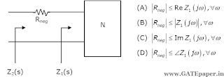
3. A negative resistance Rneg is connected to a passive network N having driving point impedance Z1(s) as shown below. For Z2(s) to be positive real,

Answer:A
Solution : https://www.youtube.com/watch?v=ESM5mIZBEeU


2008
4. The driving point impedance of the following network is given as shown. The component values are

Answer:D
Solution : https://www.youtube.com/watch?v=CI2Na_stYRg

Steady State Analysis of AC and DC circuits - Topicwise GATE Questions on Network Theory (from 2003)

2005
1. For the circuit in figure, the instantaneous current i1(t) is

Answer:A
Solution : https://www.youtube.com/watch?v=BcmlFVwT5C4


2007
2. In the AC network shown in the figure, the phasor voltage VAB(in volts) is:

Answer:D
Solution : https://www.youtube.com/watch?v=CNz1YebFlDw


2008
Common Data Questions: 3 & 4
The following series RLC circuit with zero initial conditions is excited by a unit impulse function δ(t).

3. For t > 0, the output voltage Vc(t) is

Answer:D
Solution : https://www.youtube.com/watch?v=DB4jmdoaFIk

4. For t > 0, the voltage across the resistor is

Answer:B
Solution (3 & 4) : https://www.youtube.com/watch?v=nn6PggFjKgA

2009
5. The time domain behaviour of an RL circuit is represented as shown below. For an initial current of i(0) = Vo/R, the steady state value of the current is given by

Answer:A
Solution : https://www.youtube.com/watch?v=VBFOXuUEuKE


2010
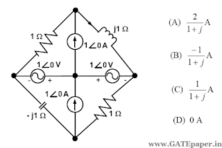
6. The current I in the circuit shown is

a) - j1 A
b) j1 A
c) 0 A
d) 20 A
Answer:A
Solution : https://www.youtube.com/watch?v=dKZILrD0vOM

2011
7. In the circuit shown below, the Norton equivalent current in amperes with respect to the terminals P and Q is

a) 6.4 - j 4.8
b) 6.56 - j 7.87
c) 10 + j 0
d) 16 + j 0


Answer:A
Solution : https://www.youtube.com/watch?v=HsLyDiBmxx4

8. The circuit shown below is driven by a sinusoidal input Vi = Vpcos(t/RC). The steady state output Vo is

Answer:A
Solution : https://www.youtube.com/watch?v=51KGart3zsQ

9. In the circuit shown below, the current I is equal to

Answer:B
Solution : https://www.youtube.com/watch?v=t9esPoyU5tY

2012
10. In the circuit shown below, the current through the inductor is

Answer:C
Solution : https://www.youtube.com/watch?v=bD4nQW3U4SA

2014
11. In the circuit shown in the figure, the value of node voltage V2 (in volts) is

a) 22 + j 2
b) 2 + j 22
c) 22 – j 2
d) 2 – j 22
Answer:D
Solution : https://www.youtube.com/watch?v=L9li2Lu26iU

12. The steady state output of the circuit shown in the figure is given by y(t) = A(ω) sin(ωt + φ(ω)).

If the amplitude |A(ω)| = 0.25, then the frequency ω is
Answer:B
Solution : https://www.youtube.com/watch?v=IIlI8e2TeDg


13. In the circuit shown in the figure,

the value of Vo(t) (in volts) for t → ∞ is ___________
Answer:31.25
Solution : https://www.youtube.com/watch?v=SHT_OgLFZmE

2015
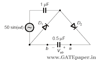
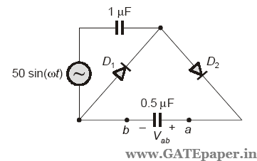
14. In the circuit shown, assume that diodes D1 and D2 are ideal. In the steady state condition, the average voltage Vab (in volts) across 0.5 µF capacitor is ____________

Answer:100
Solution : https://www.youtube.com/watch?v=2ZfO7mplk4g

Post Your Feedback (or) Doubts here.......

Name

Email *

Message *