
1987
1. Consider two energy
levels : E1, E eV above the Fermi level and E2, E eV
below the Fermi level. P1 and P2 are the probabilities of
E1 and E2 being occupied by the electron respectively.
Then
a. P1 > P2
b. P1 = P2
c. P1 < P2
d. P1 and P2
depend on number of free electrons
Answer: C
2. In an intrinsic
semiconductor, the free electron concentration depends on
a. Effective mass of electrons only
b. Effective mass of
holes only
c. Temperature of the
semiconductor
d. Width of the
forbidden energy band of the semiconductor
Answer: C
3. According to the
Einstein relation, for any semiconductor, the ratio of diffusion constant to
mobility of carriers
a. Depends upon the
temperature of the semiconductor
b. Depends upon the type
of the semiconductor
c. Varies with life time
of the semiconductor
d. Is a universal
constant
Answer: A
4. Direct band gap
semiconductors
a. Exhibit short carrier
lifetime and they are used for fabricating BJTs
b. Exhibit long carrier
lifetime and they are used for fabricating BJTs
c. Exhibit short carrier
lifetime and they are used for fabricating LASERs
d. Exhibit long carrier
lifetime and they are used for fabricating LASERs
Answer: C
1988
1989
1. Due to illumination
by light, the electron and hole concentrations in a heavily doped N-type
semiconductor increases by Δn and Δp respectively, if ni
is the intrinsic carrier concentration then
a. Δn < Δp
b. Δn > Δp
c. Δn = Δp
d. Δn x Δp = ni2
Answer: C
2. The concentration of
ionized acceptors and donors in a semiconductor are NA, ND
respectively. If NA > ND and ni is the
intrinsic concentration, then the
position of the Fermi level with respect to the intrinsic level depends on
a. NA – ND
b. NA + ND
c. (NA x ND)
/ ni2
d. ni
Answer: A
1990
1. In a semiconductor, under high electric fields, with increasing electric fields, mobility of charge carriers ............. and velocity of charge carriers ..............
Answer: Reduces, gets saturated so remains constant
Solution : http://www.youtube.com/watch?v=8cjTRCdTpbk
2. In a semiconductor
at room temperature, the intrinsic carrier concentration and resistivity are
1.5 X 10¹⁶ m-3 and 2 X 10⁵ Ω-m respectively. It
is converted into an extrinsic semiconductor with a doping concentration of 1020
per m3. For the extrinsic semiconductor, calculate the
a.
Minority carrier
concentration
b.
Resistivity
c.
Shift in Fermi level
due to doping
d.
Minority carrier concentration
when its temperature is increased to a value at which the intrinsic carrier
concentration doubles.
Assume the mobility
of majority and minority carriers to be the same and KT = 26 meV at room
temperature.
Answer:
a) 2.25 x 10¹² /m3
b) 60 Ω-m
c) 0.228 eV
d) 9 x 10¹² /m3
Solution : https://www.youtube.com/watch?v=1E491IgBz-I
1991
1.
A silicon sample is
uniformly doped with 1016 phosphorous atoms/cm3 and 2 X
1016 boron atoms/cm3. If all the dopants are fully ionized,
the material is ………..
Answer: P-type with 106 holes/cm3
2.
An n-type silicon
sample, having electron mobility µn twice the hole
mobility µp, is subjected to a steady illumination
such that the electron concentration doubles from its thermal equilibrium
value, as a result, the conductivity of the sample increases by a factor of
………..
Answer: 2
Solution :
https://www.youtube.com/watch?v=zxbCiNPkQqY
3.
The current in a
forward biased P+N junction shown in figure (a) is entirely due to
diffusion of holes from x = 0 to x = L. The injected hole concentration
distribution in the n-region is linear as shown in figure (b), with P(0) = 1022
per cm3 and L = 10-3 cm. Determine
a.
The current density
in the diode, assuming that the diffusion coefficient of holes is 12 cm2/sec.
b.
The velocity of holes
in the n-region at x = 0.

Answer:
Jn = 19.2 x 10⁶ A/cm2
υn = 12 x 103 cm/sec
Jn = 19.2 x 10⁶ A/cm2
υn = 12 x 103 cm/sec
Solution : https://www.youtube.com/watch?v=fJJ5YtXBBnA
1992
1. A semiconductor is
irradiated with light such that carriers are uniformly generated throughout its
volume. The semiconductor is n-type with ND = 1019 cm-3.
If the excess electron concentration in the steady state is Δn = 1015
cm-3 and if τp = 10 µsec (minority carrier
life time), then the generation rate due to irradiation is ………….

1993
1994
1. A small concentration
of minority carriers is injected into a homogeneous semiconductor crystal at
one point. An electric field of 10 V/cm is applied across the crystal and this
moves the minority carriers a distance of 1 cm in 20 µsec. The mobility in
cm2/volt-sec will be
a. 1000
b. 2000
c. 5000
d. 50000
Answer: C
2. A p-type silicon
sample has a higher conductivity compared to an n-type sample having the same
dopant concentration. (TRUE / FALSE)
Answer: FALSE
3. Show that the minimum
conductivity of an extrinsic silicon sample occurs when it is slightly p-type.
Calculate the electron and hole concentrations when the conductivity is
minimum. Given that µn = 1350 cm2/volt-sec, µp = 450 cm2/volt-sec,
and the intrinsic carrier concentration, ni = 1.5 X 10¹⁰
cm-3.
Answer: no = ni√µp∕µn and po = ni√µn∕µp
Solution : https://www.youtube.com/watch?v=_O5iozGDyEM
1995
1. The drift velocity of
electrons, in silicon
a. Is proportional to
the electric field for all values of electric field
b. Is independent of the
electric field
c. Increases at low
values of electric field and decreases at high values of electric field
exhibiting negative differential resistance.
d. Increases linearly
with electric field at low values of electric field and gradually saturates at
higher values of electric field.
Answer: D
2. In a p-type silicon
sample, the hole concentration is 2.25 X 1015 cm-3. If
the intrinsic carrier concentration is 1.5 X 1010 cm-3, the
electron concentration is
a. Zero
b. 1010 cm-3
c. 105 cm-3
d. 1.5 X 10¹⁰
cm-3
Answer: C
Solution : https://www.youtube.com/watch?v=j2CvMPiwMW8
3. The probability that
an electron in a metal occupies the Fermi level at any temperature T is (T >
0oK)
Answer: 1
4. In an extrinsic semiconductor, if

Answer: a-5, b-5, c-3
Solution : https://www.youtube.com/watch?v=Zk5QaYZDYbs
5. The Fermi level of
an n-type germanium film is 0.2 eV above the intrinsic Fermi level towards the
conduction band. The thickness of the
film is 0.5 µm. Calculate the sheet resistance of the film.
Assume :
ni
= 1013 cm-3,
µn
= 3500 cm2/V-sec,
µp
= 1500 cm2/V-sec,
KT/q = 26 mV.
1996
1997
1. The intrinsic carrier
density at 300oK is 1.5 X 10¹⁰ per cm3 for
silicon. For n-type silicon doped to 2.25 X 10¹⁵ atoms/cm3,
the equilibrium electron and hole densities are
Solution : https://www.youtube.com/watch?v=PCnFSBDZldQ
2. An n-type silicon bar is doped
uniformly by phosphorous atoms to a concentration 4.5 x 1013 cm-3.
The bar has cross section of 1 mm2 and length of 10 cm. It is
illuminated uniformly for region x < 0 as shown.
Assume optical
generation rate as 1021 electron-hole pairs per cm3 per
second, the hole lifetime and electron lifetime are equal to 1 µsec.
Evaluate the hole and
electron diffusion currents at x = 36.4 µm.

Answer:
Solution :
1998
1. The electron and hole
concentrations in a intrinsic semiconductor are ni and pi
respectively. When doped with a P-type material, these changes to n and p
respectively. Then
a. n + P = ni
+ Pi
b. n + ni = p
+ pi
c. npi = nip
d. np = nipi
Answer: D
Solution : https://www.youtube.com/watch?v=Zm31Ob0KekU
2. A long specimen of
p-type semiconductor material
a. Is positively charged
b. Is electrically
neutral
c. Has an electric field
directed along its length
d. Acts as a dipole
Answer: B
Solution : https://www.youtube.com/watch?v=CMnmcekH-3g
3. The units of (q/KT)
are
a. V
b. V-1
c. J
d. J/K
Answer: B
1999
2000
2001
2002
2003
1. N – Type silicon is
obtained by doping silicon with
a. Germanium
b. Aluminum
c. Boron
d. Phosphorous
Answer: D
2. The band gap of
silicon at 3000K is
a. 1.36 eV
b. 1.10 eV
c. 0.80 eV
d. 0.67 eV
Answer: B
Solutoin : https://www.youtube.com/watch?v=_NjNJR8cCEU
3. The intrinsic carrier
concentration of silicon sample at 300oK is 1.5 x 10¹⁶ m-3.
If after doping, the number of majority carriers is 5 x 10²⁰ m-3,
the minority carrier density is
a. 4.50 x 10¹¹
/m3
b. 3.33 x 10⁴
/m3
c. 5.00 x 10²⁰
/m3
d. 3.00 x 10⁻⁵
/m3
Answer: A
Solutoin : https://www.youtube.com/watch?v=csUoP33C4k4
4. An N type silicon bar
0.1 cm long and µm2 in cross sectional area
has a majority carrier concentration of 5 x 10²⁰ m-3 and
the carrier mobility is 0.13 m2/V-sec at 300oK. If the
charge of an electron is 1.6 x 10⁻¹⁹ coulomb, then the resistance of
the bar is
a. 106 Ω
b. 104 Ω
c. 10-1 Ω
d. 10-4 Ω
Answer: A
Solutoin : https://www.youtube.com/watch?v=3y_xJwMihpo
5. The electron
concentration in a sample of uniformly doped N type silicon at 300oK
varies linearly from 1017 cm-3 at x = 0 µm
to 6 x 1016 cm-3
at x = 2 µm. Assume a situation that electrons are supplied to keep this
concentration gradient constant with time. If electronic charge is 1.6 x 10⁻¹⁹
coulomb and the diffusion constant Dn = 35 cm2/sec, the
current density in the silicon, if no electric field is present is
a. Zero
b. -112 A/cm2
c. +1120 A/cm2
d. -1120 A/cm2
Answer: D
Solutoin : https://www.youtube.com/watch?v=Y5ktNfyNHW0
2004
1. The impurity commonly
used for realizing the base region of a silicon NPN transistor is
a. Gallium
b. Indium
c. Boron
d. Phosphorous
Answer: C
Solution : https://www.youtube.com/watch?v=NkcGfnAzVvE
2. The resistivity of a
uniformly doped N type silicon sample is 0.5 Ω-cm. If the electron
mobility (µn) is 1250 cm2/V-sec and the
charge of an electron is 1.6 x 10⁻¹⁹ coulomb, then the donor
impurity concentration (ND) in the sample is
a. 2 x 10¹⁶ /
cm3
b. 1 x 10¹⁶ /
cm3
c. 2.5 x 10¹⁵
/ cm3
d. 2 x 10¹⁵ /
cm3
Answer:
B Solution : https://www.youtube.com/watch?v=_bfVDPlUFWw
2005
1. The band gap of
silicon at room temperature is
a. 1.3 eV
b. 0.7 eV
c. 1.1 eV
d. 1.4 eV
Answer: C
2. The primary reason
for the widespread use of silicon in semiconductor device technology is
a. Abundance of silicon
on the surface of the earth
b. Larger band gap of
silicon in comparison to germanium
c. Favorable properties
of silicon – dioxide (SiO2)
d. Lower melting point
Answer: A
Solution : https://www.youtube.com/watch?v=6742WDMV-3U
3. A silicon sample A is
doped with 1018 atoms/cm3 of boron. Another sample B of
identical dimensions is doped with 1018 atoms/cm3 of phosphorous.
The ratio of electron to hole mobility is 3. The ratio of conductivity of the
sample A to B is
a. 3
b. 1/3
c. 2/3
d. 3/2
Answer: B
Solution : https://www.youtube.com/watch?v=4GDAybGas6c
2006
1. The concentration of
minority carriers in an extrinsic semiconductor under equilibrium is
a. Directly proportional
to the doping concentration
b. Inversely
proportional to the doping concentration
c. Directly proportional
to the intrinsic concentration
d. Inversely
proportional to the intrinsic concentration
Answer: B
Solution : https://www.youtube.com/watch?v=iujDfqtrnyA
2. Under low level
injection assumption, the injected minority carrier current for an extrinsic
semiconductor is essentially the
a. Diffusion current
b. Drift current
c. Recombination current
d. Induced current
Answer: A
Solution : https://www.youtube.com/watch?v=TYB5k5Y48t4
3. The majority carriers
in an N-type semiconductor have an average drift velocity V in a direction perpendicular to a uniform magnetic field B. The electric field E induced due to hall effect acts in
the direction

Solution : https://www.youtube.com/watch?v=auzgCSNqVcU
4. A heavily doped
N-type semiconductor has the following data:
Hole – electron
mobility ratio : 0.4
Doping concentration :
4.2 x 10⁸ /m3
Intrinsic
concentration :
1.5 x 10⁴ /m3
The ratio of
conductance of the N-type semiconductor to that of the intrinsic semiconductor
of same material and at the same temperature is given by
a. 0.00005
b. 2000
c. 10000
d. 20000
Answer: D
Solution : https://www.youtube.com/watch?v=NmYZgSc58Gw
2007
1. The electron and hole
concentrations in an intrinsic semiconductor are ni per cm3
at 300oK. Now if acceptor impurities are introduced with a
concentration of NA per cm3 (where NA > ni),
then electron concentration per cm3 at 300oK will be
a. ni
b. ni + NA
c. NA – ni
d. ni2
/ NA
Answer: D
Solution : https://www.youtube.com/watch?v=gwb5IZFKDw0
2008
1. Which of the
following is TRUE?
a. A silicon wafer
heavily doped with boron is a P+ substrate
b. A silicon wafer lightly
doped with boron is a P+ substrate
c. A silicon wafer
heavily doped with Arsenic is a P+ substrate
d. A silicon wafer
lightly doped with Arsenic is a P+ substrate
Answer: A
Solution : https://www.youtube.com/watch?v=wWLqWJ5JX3U
2. Silicon is doped with
boron to a concentration of 4x10¹⁷atoms/cm3. Assuming the
intrinsic carrier concentration of silicon to be 1.5x1010 cm-3
and the value of KT/q to be 25 mV at 300oK. Compared to undoped
silicon, the Fermi level of doped silicon
a. Goes down by 0.13 eV
b. Goes up by 0.13 eV
c. Goes down by 0.427 eV
d. Goes up by 0.427 eV
Answer: C
Solution : https://www.youtube.com/watch?v=B4keN9lEFS8
2009
1. In an N type silicon
crystal at room temperature, which of the following can have a concentration of
4x1019 cm-3?
a. Silicon atoms
b. Holes
c. Dopant atoms
d. Valence electrons
Answer: C
Solution : https://www.youtube.com/watch?v=ck2TRWxTGGM
2. The ratio of the
mobility to the diffusion coefficient in a semiconductor has the units
a. V-1
b. cm. V-1
c. V. cm-1
d. V.sec
Answer: A
Solution : https://www.youtube.com/watch?v=CbvKuwdmwPY
2010
1. Linked Answer
Question:
The silicon sample
with unit cross sectional area shown below is in thermal equilibrium. The
following information is given:
T = 300oK
Electron charge =
1.6x10⁻¹⁹ C
Thermal voltage = 26
mV
Electron mobility =
1350 cm2/volt-sec

i.
The magnitude of the
electric field at x = 0.5 µm is
a. 1 KV/cm
b. 5 KV/cm
c. 10 KV/cm
d. 26 KV/cm
Answer: C
ii.
The magnitude of the
electron drift current density at x = 0.5 µm is
a. 2.16x10⁴
A/cm2
b. 1.08x10⁴
A/cm2
c. 4.32x10³
A/cm2
d. 6.48x10²
A/cm2
Answer: A
Solution : https://www.youtube.com/watch?v=jLAgBiAE4so
2011
1. Drift current in
semiconductors depends upon
a. Only the electric
field
b. Only the carrier
concentration gradient
c. Both the electric
field and the carrier concentration
d. Both the electric
field and the carrier concentration gradient
Answer: C
Solution : https://www.youtube.com/watch?v=fArk1NqX5pU
2012
2013
2014
Set – 1
(15th February 2014 (Forenoon))
SET – 2
(15th February 2014 (Afternoon))
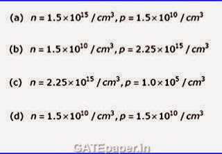
1. A silicon bar is
doped with donor impurities ND = 2.25 x 10¹⁵ atoms/cm3.
Given the intrinsic carrier concentration of silicon at T = 300oK is
ni = 1.5 x 1010 cm-3. Assuming complete
impurity ionization, the equilibrium electron and hole concentrations are
a. no = 1.5 x
1016 cm-3, p0 = 1.5 x 105 cm-3
b. no = 1.5 x
1010 cm-3, p0 = 1.5 x 1015 cm-3
c. no = 1.5 x
1015 cm-3, p0 = 1.5 x 1010 cm-3
d. no = 1.5 x
1015 cm-3, p0 = 1.5 x 105 cm-3
Answer: D
Solution : https://www.youtube.com/watch?v=zvQFdUBhINg
2. Assume electron
charge q = 1.6 x 10⁻¹⁹C, KT/q = 25 mV and electron mobility µn = 1000 cm2/volt-sec.
If the concentration gradient of electrons injected into a P type silicon
sample is 1 x 10²¹ per cm-3, the magnitude of electron
diffusion current density (in A/cm2) is ………….
Answer: 4000
Solution : https://www.youtube.com/watch?v=IBb_zfgQ1AY
SET –
3 (16th February 2014 (Forenoon))
1. A thin P type silicon
sample is uniformly illuminated with light which generates excess carriers. The
recombination rate is directly proportional to
a. The minority carrier
mobility
b. The minority carrier
recombination lifetime
c. The majority carrier
concentration
d. The excess minority
carrier concentration
Answer: D
2. At T = 300oK,
the hole mobility of a semiconductor µp = 500 cm2/volt-sec
and KT/q = 26 mV. The hole diffusion constant Dp in cm2/sec
is ………
Answer: 13
SET - 4 (16th February 2014 (Afternoon))
1. In the figure, ln(ρi) is plotted as a
function of 1/T, where ρi is the intrinsic resistivity of
silicon, T is the temperature, and the plot is almost linear. The slope of the
line can be used to estimate

a. Band gap energy of
silicon
b. Sum of electron and
hole mobility in silicon
c. Reciprocal of the sum
of electron and hole mobility in silicon
d. Intrinsic carrier
concentration of silicon
Answer: A
2. Consider a silicon
sample doped with ND = 1 x 10¹⁵ /cm3 donor
atoms. Assume that the intrinsic carrier concentration ni = 1.5 x 1010 cm-3. If the
sample is additionally doped with NA = 1 x 1018 cm-3
acceptor atoms, the approximate number of electrons /cm3 in the
sample, at T = 300oK, will be…………
Answer: 225
3. An N type
semiconductor having uniform doping is biased as shown in the figure.

Answer: D
2015
2015
1.
A silicon sample is uniformly doped with donor type impurities with a
concentration of 1016 cm-3. The electron and hole
mobilities in the sample are 1200 cm2/V-sec and 400 cm2/V-sec
respectively. Assume complete ionization of impurities. The charge of an
electron is 1.6x10⁻¹⁹ C. The resistivity of the sample (in
Ω-cm) is _______________
Answer: 0.52
Solution : https://www.youtube.com/watch?v=Zo6ei-B4gX8
Answer: 0.52
Solution : https://www.youtube.com/watch?v=Zo6ei-B4gX8
2. A piece of
silicon is doped uniformly with phosphorous with a doping concentration of 1016
per cm3. The expected value of mobility verses doping concentration for
silicon assuming full dopant ionization is shown below. The charge of an
electron is 1.6x10⁻¹⁹ C. The conductivity (in Simons/cm) of
the silicon sample at 300oK is _______________

3. An N-type
silicon sample is uniformly illuminated with light which generates 1020
electron-hole pairs per cm3 per second. The minority carrier
lifetime in the sample is 1 µs. In the steady state, the hole concentration in
the sample is approximately 10x, where x is an integer. The value of
x is _________________
Answer: 14
Solution : https://www.youtube.com/watch?v=Cd_4k0VGFXg
Answer: 14
Solution : https://www.youtube.com/watch?v=Cd_4k0VGFXg
4. The energy band
diagram and the electron density profile n(x) in a semiconductor are shown in
the figures.

5. A DC voltage of
10 volts is applied across an N-type silicon bar having a rectangular cross
section and length of 1 cm as shown. The donor doping concentration ND
and the mobility of electron µn are 1016 cm-3
and 1000 cm2/V-sec respectively. The average time (in µs) taken by
the electrons to move from one end of the bar to the other end is
_______________

can anyone help me solving 1997 the figure one 2nd question or provide the link for that
ReplyDeletesame here
DeleteAt 300 K, if acceptor density in a semiconductor is 1018 cm-3 while the intrinsic carrier concentration is 1010 cm-3, then the difference between the Fermi level of doped semiconductor and the intrinsic Fermi level is:
ReplyDeleteWhen your website or blog goes live for the first time, it is exciting. That is until you realize no one but you and your. read more
ReplyDeleteWow! Such an amazing and helpful post this is. I really really love it. It's so good and so awesome. I am just amazed. I hope that you continue to do your work like this in the future also buy bad Facebook reviews
ReplyDeleteThis is a great inspiring article.I am pretty much pleased with your good work.You put really very helpful information... Pregnancy test strips
ReplyDeleteIts a good compilation
ReplyDeleteYou there, this is really good post here. Thanks for taking the time to post such valuable information. Quality content is what always gets the visitors coming. cookie sheet
ReplyDeleteNice blog, I will keep visiting this blog very often. chicago med season 5
ReplyDeleteYou are not limited to only certain set of exercises. Resistance Bands
ReplyDeleteYou completed a few fine points there. I did a search on the subject and found nearly all persons will go along with with your blog. belk mattress topper
ReplyDeleteCool stuff you have got and you keep update all of us. belk mattress topper
ReplyDeleteTruly, this article is really one of the very best in the history of articles. I am a antique ’Article’ collector and I sometimes read some new articles if I find them interesting. And I found this one pretty fascinating and it should go into my collection. Very good work! Hawaii car transport
ReplyDeleteThank you for some other informative blog. Where else could I get that type of information written in such an ideal means? I have a mission that I’m just now working on, and I have been at the look out for such information. Escort
ReplyDeleteYou should mainly superior together with well-performing material, which means that see it: הסכם עבודה עם קבלן מפתח
ReplyDeletein question no 4 .....https://www.youtube.com/watch?v=oibHxv4SAs8....
ReplyDeleteaccording to your solution the ans of this question is 2.2*(10)^-2...but i think ans is wrong because,the concentration of doping is not uniform throughout the SC, thus to maintain the equilibrium internal electric field is generated due to which the band of the SC is varying with slope -0.1eV/cm.
the generated electric field opposes the diffusion of carriers due to concentration gradient and thus there will be no current flow inside the SC.
sir, 2010 paper you have taken electron concn as 10^6 but in the problem it is given as 10^16
ReplyDeleteThank you the paper. This will definetely helpful.
ReplyDeleteFlipkart Standard Chartered Offers
In a few earlier cases, laborers in closeness to a swinging or sliding gate administrator have gotten caught and squashed by the engine regulator and the activity of the joined intention arm or drive chain systems. autogate swing arm
ReplyDeleteSimply great!!!
ReplyDeleteThank you
ReplyDelete